
Datasheet


AS4C32M16D1A-C&I
1
Rev. 1.0 Mar. /2015
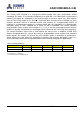
Pin Descriptions
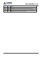
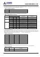
Table 2. Pin Details
Symbol
Type
Description
CK,
CK
Input
Differential Clock: CK and
CK
are differential clock inputs. All address and control
input signals are sampled on the crossing of the positive edge of CK and negative
edge of
CK
. Input and output data is referenced to the crossing of CK and
CK
(both
directions of the crossing)
CKE
Input
Clock Enable: CKE activates (HIGH) and deactivates (LOW) the CK signal. If CKE
goes low synchronously with clock, the internal clock is suspended from the next clock
cycle and the state of output and burst address is frozen as long as the CKE remains
low. When all banks are in the idle state, deactivating the clock controls the entry to
the Power Down and Self Refresh modes.
BA0, BA1
Input
Bank Activate: BA0 and BA1 define to which bank the BankActivate, Read, Write, or
BankPrecharge command is being applied.
A0-A12
Input
Address Inputs: A0-A12 are sampled during the BankActivate command (row
address A0-A12) and Read/Write command (column address A0-A9 with A10 defining
Auto Precharge).
CS
Input
Chip Select:
CS
enables (sampled LOW) and disables (sampled HIGH) the
command decoder. All commands are masked when
CS
is sampled HIGH.
CS
provides for external bank selection on systems with multiple banks. It is considered
part of the command code.
RAS
Input
Row Address Strobe: The
RAS
signal defines the operation commands in
conjunction with the
CAS
and
WE
signals and is latched at the positive edges of CK.
When
RAS
and
CS
are asserted "LOW" and
CAS
is asserted "HIGH," either the
BankActivate command or the Precharge command is selected by the
WE
signal.
When the
WE
is asserted "HIGH," the BankActivate command is selected and the
bank designated by BA is turned on to the active state. When the
WE
is asserted
"LOW," the Precharge command is selected and the bank designated by BA is
switched to the idle state after the precharge operation.
CAS
Input
Column Address Strobe: The
CAS
signal defines the operation commands in
conjunction with the
RAS
and
WE
signals and is latched at the positive edges of CK.
When
RAS
is held "HIGH" and
CS
is asserted "LOW," the column access is started
by asserting
CAS
"LOW." Then, the Read or Write command is selected by asserting
WE
"HIGH" or “LOW”.
WE
Input
Write Enable: The
WE
signal defines the operation commands in conjunction with
the
RAS
and
CAS
signals and is latched at the positive edges of CK. The
WE
input
is used to select the BankActivate or Precharge command and Read or Write
command.
LDQS,
UDQS
Input /
Output
Bidirectional Data Strobe: Specifies timing for Input and Output data. Read Data
Strobe is edge triggered. Write Data Strobe provides a setup and hold time for data
and DQM. LDQS is for DQ0~7, UDQS is for DQ8~15.
LDM,
UDM
Input
Data Input Mask: Input data is masked when DM is sampled HIGH during a write
cycle. LDM masks DQ0-DQ7, UDM masks DQ8-DQ15.
DQ0 - DQ15
Input /
Output
Data I/O: The DQ0-DQ15 input and output data are synchronized with positive and
negative edges of LDQS and UDQS. The I/Os are byte-maskable during Writes.
V
DD
Supply
Power Supply: 2.5V
±
0.2V .