
Datasheet


AS4C32M16D1A-C&I
40
Rev. 1.0 Mar. /2015
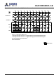
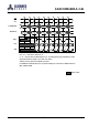
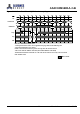
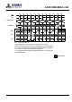
Figure 23. Write to Read Max tDQSS, ODD Number of Data, Interrupting
CK
CK
WRITE
NOP NOP
READ
Bank
Col n
ADDRESS
T0 T1 T2 T3
T4
T5 T6 T7
T8 T9
NOP
DQS
DQ
tDQSS (max)
DM
DI
n
Bank
Col o
T10 T11
NOP
tWTR
CL=3
Don’t Care
DI n = Data In for column n
tWTR is referenced from the first positive CK edge after the last Data In Pair (not the last desired
Data In element)
DM= LDM & UDM
An interrupted burst of 8 is shown, 1 data elements are written
A10 is LOW with the WRITE command (AUTO PRECHARGE is disabled)
The READ and WRITE commands are to the same devices but not necessarily to the same bank
T12
COMMAND