
Datasheet


AS4C32M16D1A-C&I
10
Rev. 1.0 Mar. /2015
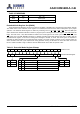
Table 17. Recommended A.C. Operating Conditions
(V
DD
= 2.5V ± 0.2V, T
A
= -40~85 C)
Symbol
Parameter
Min.
Max.
Unit
V
IH
(AC)
Input High Voltage (AC)
V
REF
+ 0.31
-
V
V
IL
(AC)
Input Low Voltage (AC)
-
V
REF
– 0.31
V
V
ID
(AC)
Input Different Voltage, CK and
CK
inputs
0.7
V
DDQ +
0.6
V
V
IX
(AC)
Input Crossing Point Voltage, CK and
CK
inputs
0.5*V
DDQ
-0.2
0.5*V
DDQ
+0.2
V
Note:
1) Enables on-chip refresh and address counters.
2) Min(t
CL
, t
CH
) refers to ther smaller of the actual clock low time and actual clock high time as provided to the device.
3) t
HZ
and t
LZ
transitions occur in the same access time windows as valid data transitions. These parameters are not
referenced to a specific voltage level, but specify when the device output is no longer driving(HZ), or begins
driving(LZ).
4) The specific requirement is that DQS be valid (High, Low, or at some point on a valid transition) on or before this
CLK edge. A valid transition is defined as monotonic, and meeting the input slew rate specifications of the device.
When no writes were previously in progress on the bus, DQS will be transitioning from High-Z to logic LOW. If a
previous write was in progress, DQS could be HIGH, LOW, or transitioning from HIGH to LOW at this time,
depending on t
DQSS
.
5) The maximum limit for this parameter is not a device limit. The device will operate with a greater value for this
parameter, but system performance (bus turnaround) will degrade accordingly.
6) For command/address and CK &
CK
slew rate
≧
1.0V/ns.
7) A maximum of eight AUTO REFRESH commands can be posted to any given DDR SDRAM device.
8) Power-up sequence is described in Note 10
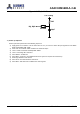
9) A.C. Test Conditions
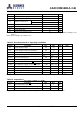
Table 18. SSTL _2 Interface
Reference Level of Output Signals (V
REF
)
0.5 * V
DDQ
Output Load
Reference to the Test Load
Input Signal Levels
V
REF
+0.31 V / V
REF
-0.31 V
Input Signals Slew Rate
1 V/ns
Reference Level of Input Signals
0.5 * V
DDQ