
Datasheet


AS4C32M16D1A-C&I
9
Rev. 1.0 Mar. /2015
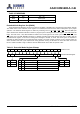
Table 16. Electrical Characteristics and Recommended A.C.Operating Condition
(V
DD
= 2.5V ± 0.2V, T
A
= -40~85 C)
Symbol
Parameter
-5
Unit
Note
Min.
Max.
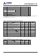
t
CK
Clock cycle time
CL = 2
7.5
12
ns
CL = 2.5
6
12
ns
CL = 3
5
12
ns
t
CH
Clock high level width
0.45
0.55
t
CK
t
CL
Clock low level width
0.45
0.55
t
CK
t
HP
Clock half period
t
CLMIN
or t
CHMIN
-
ns
2
t
HZ
Data-out-high impedance time from CK,
CK
-
0.7
ns
3
t
LZ
Data-out-low impedance time from CK,
CK
-0.7
0.7
ns
3
t
DQSCK
DQS-out access time from CK,
CK
-0.6
0.6
ns
t
AC
Output access time from CK,
CK
-0.7
0.7
ns
t
DQSQ
DQS-DQ Skew
-
0.4
ns
t
RPRE
Read preamble
0.9
1.1
t
CK
t
RPST
Read postamble
0.4
0.6
t
CK
t
DQSS
CK to valid DQS-in
0.72
1.25
t
CK
t
WPRES
DQS-in setup time
0
-
ns
4
t
WPRE
DQS Write preamble
0.25
-
t
CK
t
WPST
DQS write postamble
0.4
0.6
t
CK
5
t
DQSH
DQS in high level pulse width
0.35
-
t
CK
t
DQSL
DQS in low level pulse width
0.35
-
t
CK
t
IS
Address and Control input setup time
0.7
-
ns
6
t
IH
Address and Control input hold time
0.7
-
ns
6
t
DS
DQ & DM setup time to DQS
0.4
-
ns
t
DH
DQ & DM hold time to DQS
0.4
-
ns
t
QH
DQ/DQS output hold time from DQS
t
HP
- t
QHS
-
ns
t
RC
Row cycle time
55
-
ns
t
RFC
Refresh row cycle time
70
-
ns
t
RAS
Row active time
40
70K
ns
t
RCD
Active to Read or Write delay
15
-
ns
t
RP
Row precharge time
15
-
ns
t
RRD
Row active to Row active delay
10
-
ns
t
WR
Write recovery time
15
-
ns
t
WTR
Internal Write to Read Command Delay
2
-
t
CK
t
MRD
Mode register set cycle time
10
-
ns
t
REFI
Average Periodic Refresh interval
-
7.8
s
7
t
XSRD
Self refresh exit to read command delay
200
-
t
CK
t
XSNR
Self refresh exit to non-read command delay
75
-
ns
t
DAL
Auto Precharge write recovery + precharge time
t
WR
+t
RP
-
ns
t
DIPW
DQ and DM input pulse width
1.75
-
ns
t
IPW
Control and Address input pulse width
2.2
-
ns
t
QHS
Data Hold Skew Factor
-
0.5
ns
t
DSS
DQS falling edge to CK setup time
0.2
-
t
CK
t
DSH
DQS falling edge hold time from CK
0.2
-
t
CK