
Datasheet


AS4C32M16D1A-C&I
7
Rev. 1.0 Mar. /2015
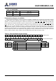
Table 12. Absolute Maximum Rating
Symbol
Item
Values
Unit
V
IN
, V
OUT
Input, Output Voltage
- 0.5~ V
DDQ
+ 0.5
V
V
DD
, V
DDQ
Power Supply Voltage
- 1~3.6
V
T
A
Ambient Temperature
Commercial
0~70
°
C
Industrial
-40~85
°
C
T
STG
Storage Temperature
- 55~150
°
C
T
SOLDER
Soldering Temperature
260
°
C
P
D
Power Dissipation
1
W
I
OS
Short Circuit Output Current
50
mA
Note1: Stress greater than those listed under "Absolute Maximum Ratings" may cause permanent damage to the
device.
Note2: These voltages are relative to Vss
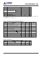
Table 13. Recommended D.C. Operating Conditions
Symbol
Parameter
Min.
Max.
Unit
Note
V
DD
Power Supply Voltage
2.3
2.7
V
V
DDQ
Power Supply Voltage (for I/O Buffer)
2.3
2.7
V
V
REF
Input Reference Voltage
0.49*V
DDQ
0.51* V
DDQ
V
V
IH
(DC)
Input High Voltage (DC)
V
REF
+ 0.15
V
DDQ
+ 0.3
V
V
IL
(DC)
Input Low Voltage (DC)
-0.3
V
REF
– 0.15
V
V
TT
Termination Voltage
V
REF
- 0.04
V
REF
+ 0.04
V
V
IN
(DC)
Input Voltage Level, CK and
CK
inputs
-0.3
V
DDQ
+ 0.3
V
V
ID
(DC)
Input Different Voltage, CK and
CK
inputs
0.36
V
DDQ
+ 0.6
V
I
I
Input leakage current
-2
2
A
I
OZ
Output leakage current
-5
5
A
I
OH
Output High Current
-16.2
-
mA
V
OH
= 1.95V
I
OL
Output Low Current
16.2
-
mA
V
OL
= 0.35V
Note : All voltages are referenced to V
SS
.
Table 14. Capacitance
(V
DD
= 2.5V, f = 1MHz, T
A
= 25 C)
Symbol
Parameter
Min.
Max.
Unit
C
IN1
Input Capacitance (CK,
CK
)
2
3
pF
C
IN2
Input Capacitance (All other input-only pins)
2
3
pF
C
I/O
DQ, DQS, DM Input/Output Capacitance
4
5
pF
Note: These parameters are guaranteed by design, periodically sampled and are not 100% tested