
Datasheet
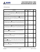


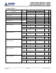

DQ and DM input setup time
(VIH/VIL (AC) levels)
1.35V
t
DS
(base)
AC135
25 - ps
17
1.5V
t
DS
(base)
AC150
10 - ps
17
Control and Address Input pulse width
for each input
t
IPW
560 - ps
25
DQ and DM Input pulse width
for each input
t
DIPW
360 - ps
25
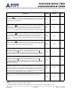
DQ high impedance time t
HZ
(DQ) - 225 ps
13,14
DQ low impedance time t
LZ
(DQ) -450 225 ps
13,14
DQS, DQS high impedance time
(RL + BL/2 reference)
t
HZ
(DQS) - 225 ps
13,14
DQS, DQS low impedance time
(RL - 1 reference)
t
LZ
(DQS) -450 225 ps
13,14
DQS, DQS to DQ Skew,
per group, per access
t
DQSQ
- 100 ps
12,13
CAS to CAS command delay t
CCD
4 - nCK
DQ output hold time from DQS, DQS
t
QH
0.38 - t
CK
(avg)
12,13
DQS, DQS rising edge output
access time from rising CK, CK
t
DQSCK
-225 225 ps
12,13
DQS latching rising transitions
to associated clock edges
t
DQSS
-0.27 0.27 t
CK
(avg)
DQS falling edge hold time
from rising CK
t
DSH
0.18 - t
CK
(avg)
29
DQS falling edge setup time
to rising CK
t
DSS
0.18 - t
CK
(avg)
29
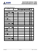
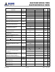
DQS input high pulse width t
DQSH
0.45 0.55 t
CK
(avg)
27,28
DQS input low pulse width t
DQSL
0.45 0.55 t
CK
(avg)
26,28
DQS output high time t
QSH
0.40 - t
CK
(avg)
12,13
DQS output low time t
QSL
0.40 - t
CK
(avg)
12,13
Mode register set command cycle time t
MRD
4 - nCK
Mode register set command update
delay
t
MOD
15 - ns
12 - nCK
Read preamble time t
RPRE
0.9 - t
CK
(avg)
13,19
Read postamble time t
RPST
0.3 - t
CK
(avg)
11,13
Write preamble time t
WPRE
0.9 - t
CK
(avg)
1
Write postamble time t
WPST
0.3 - t
CK
(avg)
1
Write recovery time t
WR
15 - ns
Auto precharge write recovery
+ Precharge time
t
DAL
(min) WR + roundup [tRP / tCK(avg)] nCK
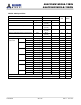
Parameter Symbol
- 12 (DDR3L-1600)
Unit NoteMin Max
AS4C256M16D3LB-12BIN
AS4C256M16D3LB-12BCN
Confidential
- 39 of 46 -
Rev.1.1 Jan. 2017