
Datasheet
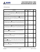


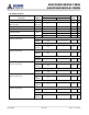

Parameter Symbol
- 12 (DDR3L-1600)
Unit Note
Min
Max
Average clock cycle time t
CK
(avg)
Please refer Speed Bins
ps
Minimum clock cycle time
(DLL-off mode)
t
CK
(DLL-off)
8
-
ns
6
Average CK high level width t
CH
(avg)
0.47
0.53
t
CK
(avg)
Average CK low level width t
CL
(avg)
0.47
0.53
t
CK
(avg)
Active Bank A to Active Bank B
command period
t
RRD
7.5
-
ns
4
-
nCK
Four activate window t
FAW
40
-
ns
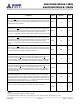
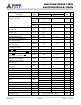
Address and Control input hold time
(VIH/VIL (DC) levels)
1.35V
t
IH
(base)
DC90
130
-
ps
16
1.5V
t
IH
(base)
DC100
120
-
ps
16
Address and Control input setup time
(VIH/VIL (AC) levels)
1.35V
t
IS
(base)
AC160
60
-
ps
16
1.5V
t
IS
(base)
AC175
45
-
ps
16
Address and Control input setup time
(VIH/VIL (AC) levels)
1.35V
t
IS
(base)
AC135
185
-
ps
16
1.5V
t
IS
(base)
AC150
170
-
ps
16,24
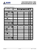
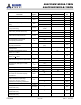
DQ and DM input hold time
(VIH/VIL (DC) levels)
1.35V
t
DH
(base)
DC90
55
-
ps
17
1.5V
t
DH
(base)
DC100
45
-
ps
17
DQ and DM input setup time
(VIH/VIL (AC) levels)
1.35V
t
DS
(base)
AC160
-
-
ps
17
1.5V
t
DS
(base)
AC175
-
-
ps
17
AC Characteristics
AS4C256M16D3LB-12BIN
AS4C256M16D3LB-12BCN
Confidential
- 38 of 46 -
Rev.1.1 Jan. 2017