
Datasheet
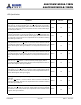
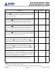

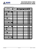

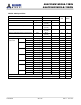
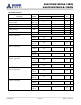
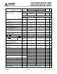
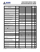

NOTE :
1. Although the DM pin has different functions, the loading matches DQ and DQS
2. This parameter is not subject to production test. It is verified by design and characterization. The capacitance is mea-
sured according to JEP147("PROCEDURE FOR MEASURING INPUT CAPACITANCE USING A VECTOR NETWORK
ANALYZER( VNA)") with VDD, VDDQ, VSS, VSSQ applied and all other pins floating (except the pin under test, CKE,
RESET
and ODT as necessary). VDD=VDDQ=1.5V, VBIAS=VDD/2 and on-die termination off.
3. This parameter applies to monolithic devices only; stacked/dual-die devices are not covered here
4. Absolute value of CCK-CCK
5. Absolute value of CIO(DQS)-CIO(DQS)
6. CI applies to ODT, CS, CKE, A0-A15, BA0-BA2, RAS, CAS, WE
7. CDI_CTRL applies to ODT, CS and CKE
8. CDI_CTRL=CI(CTRL)-0.5*(CI(CLK)+CI(CLK
))
9. CDI_ADD_CMD applies to A0-A15, BA0-BA2, RAS, CAS and WE
10. CDI_ADD_CMD=CI(ADD_CMD) - 0.5*(CI(CLK)+CI(CLK))
11. CDIO=CIO(DQ,DM) - 0.5*(CIO(DQS)+CIO(DQS
))
12. Maximum external load capacitance on ZQ pin: 5pF
AS4C256M16D3LB-12BIN
AS4C256M16D3LB-12BCN
Confidential
- 35 of 46 -
Rev.1.1 Jan. 2017