
Datasheet
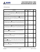


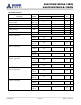

NOTE :
1) Burst Length: BL8 fixed by MRS: set MR0 A[1,0]=00B
2) Output Buffer Enable: set MR1 A[12] = 0B; set MR1 A[5,1] = 01B; RTT_Nom enable: set MR1 A[9,6,2] = 011B;
Active Standby Current; CKE: High; External clock: On; tCK, CL: see timing used table;
BL: 8; AL: 0; CS
: stable at 1; Command, Address: partially toggling; Data IO: FLOATING;
DM: stable at 0; Bank Activity: all banks open; Output Buffer and RTT: Enabled in Mode
Registers; ODT Signal: stable at 0
IDD3N
32
mA
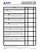
Operating Burst Read Current; CKE: High; External clock: On; tCK, CL: see timing used
table; BL: 8; AL: 0; CS: High between RD; Command, Address: partially toggling; Data
IO: seamless read data burst with di
fferent data between one burst and the next one; DM:
stable at 0; Bank Activity: all banks open, RD commands cycling through banks:
0,0,1,1,2,2,...; Output Buffer and RTT: Enabled in Mode Registers; ODT Signal: stable at 0
IDD4R
135
mA
Operating Burst Write Current; CKE: High; External clock: On; tCK, CL: see timing used
table; BL: 8; AL: 0; CS: High between WR; Command, Address: partially toggling; Data
IO: seamless write data burst with different data
between one burst and the next one; DM:
stable at 0; Bank Activity: all banks open, WR commands cycling through banks:
0,0,1,1,2,2,...; Output Buffer and RTT: Enabled in Mode Registers; ODT Signal: stable at
HIGH
IDD4W
150
mA
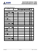
Burst Refresh Current; CKE: High; External clock: On; tCK, CL, nRFC: see timing used
table; BL: 8; AL: 0; CS
: High between REF; Command, Address: partially toggling; Data
IO: FLOATING; DM:stable at 0; Bank Activity: REF command every nRFC; Output Buffer
and RTT: Enabled in Mode Registers; ODT Signal: stable at 0
IDD5B
160
mA
Self Refresh Current: Normal Temperature Range; TCASE: 0- 85°C; Auto Self-Re-
fresh (ASR): Disabled; Self-Refresh Temperature Range (SRT): Normal; CKE: Low; Ex-
ternal clock: Off; CK and CK
: LOW; CL: see timing used table; BL: 8; AL: 0; CS,
Command, Address, Data IO: FLOATING; DM: stable at 0; Bank Activity: Self-Refresh op-
eration; Output Buffer and RTT: Enabled in Mode Registers; ODT Signal: FLOATING
IDD6
12
mA
Self Refresh Current: Extended Temperature Range; TCASE: 0- 95°C; Auto Self-Re-
fresh (ASR): Disabled; Self-Refresh Temperature Range (SRT): Extended; CKE: Low; Ex-
ternal clock: Off; CK and CK
: LOW; CL: see timing used table; BL: 8; AL: 0; CS,
Command, Address, Data IO: FLOATING; DM: stable at 0; Bank Activity: Extended Tem-
perature Self-Refresh operation; Output Buffer and RTT: Enabled in Mode Registers;
ODT Signal: FLOATING
IDD6ET
17
mA
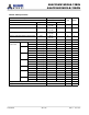
Operating Bank Interleave Read Current; CKE: High; External clock: On; tCK, nRC,
nRAS, nRCD, nRRD, nFAW, CL: see timing used table; BL: 8; AL: CL-1; CS: High be-
tween ACT and RDA; Command, Address: partially toggling; Data IO: read data bursts
with different data between one burst and the next one; DM: stable at 0; Bank Activity: two
times interleaved cycling through banks (0, 1, ...7) with different addressing; Output Buffer
and RTT: Enabled in Mode Registers; ODT Signal: stable at 0
IDD7
195
mA
RESET Low Current; RESET: Low; External clock: off; CK and CK: LOW; CKE: FLOAT-
ING; CS, Command, Address, Data IO: FLOATING; ODT Signal : FLOATING
IDD8
12
mA
Conditions Symbol IDD max. Unit
AS4C256M16D3LB-12BIN
AS4C256M16D3LB-12BCN
Confidential
- 32 of 46 -
Rev.1.1 Jan. 2017