
Datasheet
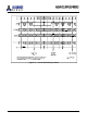
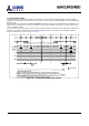
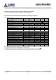
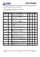
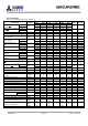
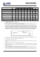

PARAMETER SYMBOL
- 5
- 6
- 75
UNIT NOTES
MIN
MAX
MIN
MAX
MIN
MAX
PRECHARGE command period
tRP
3
3
3
tCK
ACTIVE bank A to ACTIVE bank B delay
tRRD
10
12
15
ns
WRITE recovery time
tWR
15
15
15
ns
24
Auto precharge write recovery + precharge
time
tDAL
- - -
tCK 25
Internal write to Read command delay
tWTR
2
2
1
tCK
Self Refresh exit to next valid command
delay
tXSR 120 120 120 ns 26
Exit power down to next valid command
delay
tXP 2 1 1 tCK 27
CKE min. pulse width (high and low pulse
width)
tCKE 1 1 1 tCK
Refresh Period
tREF
64
64
64
ms
Average periodic refresh interval (x16)
tREFI
7.8
7.8
7.8
ȝs
28,29
Notes:
1. All voltages referenced to VSS.
2. All parameters assume proper device initialization.
3. Tests for AC timing may be conducted at nominal supply voltage levels, but the related specifications and device
operation are guaranteed for the full voltage and temperature range specified.
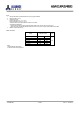
4. The circuit shown below represents the timing reference load used in defining the relevant timing parameters of the part.
It is not intended to be either a precise repres
entation of the typical system environment nor a depiction of the actual load
presented by a production tester. System designers will use IBIS or other simulation tools to correlate the timing
reference load to system environment. Manufacturers will correlate to their production test conditions (generally a coaxial
transmission line terminated at the tester electronics). For the half strength driver with a nominal 10pF load parameters
tAC and tQH are expected to be in the same range. However, these parameters are not subject to production test but are
estimated by design / characterization. Use of IBIS or other simulation tools for system design valida
tion is suggested.
5. The CK/ CK input reference voltage level (for timing referenced to CK/ CK ) is the point at which CK and CK cross; the
input reference voltage level for signals other than CK/
CK is VDDQ/2.
6. The timing reference voltage level is VDDQ/2.
7. AC and DC input and output voltage levels are defined in the section for Electrical Characteristics and AC/DC operating
conditions.
8. A CK/ CK differential slew rate of 2.0 V/ns is assumed for all parameters.
9. CAS latency definition: with CL = 3 the first data element is valid at (2 * tCK + tAC) after the clock at which the READ
command was registered; with CL = 2 the first data element is valid at (tCK + tAC) after the clock at which the READ
command was registered
10. Min (tCL, tCH) refers to
the smaller of the actual clock low time and the actual clock high time as provided to the device
(i.e. this value can be greater than the minimum specification limits of tCL and tCH)
11. tQH = tHP - tQHS, where tHP = minimum half clock period for any given cycle and is defined by clock high or clock low
(tCL, tCH). tQHS accounts for 1) the pulse duration distortion of on-chip clock circuits; and 2) the worst case push-out of
AS4C16M16MD1
256Mb MOBILE DDR SDRAM
Confidential
- 49/56 -
Ver.1.1 Oct.2015