
Datasheet
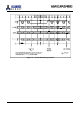
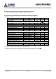

8.4 IDD Specification Parameters and Test Conditions
8.4.1 IDD Specification Parameters and Test Conditions
[Recommended Operating Conditions; Notes 1-3]
(256Mb, X16)
PARAMETER
SYMBOL
TEST CONDITION
-5
- 6
- 75
UNIT
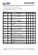
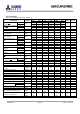
Operating one
bank active-
precharge current
IDD0
tRC = tRCmin ; tCK = tCKmin ; CKE is HIGH; CS is HIGH
between valid commands; address inputs are
SWITCHING; data bus inputs are STABLE
40 38 35 mA
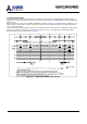
Precharge power-
down standby
current
IDD2P
all banks idle, CKE is LOW; CS is HIGH, tCK = tCKmin ;
address and control inputs are SWITCHING; data bus
inputs are STABLE
0.4 0.4 0.4 mA
Precharge power-
down standby
current with clock
stop
IDD2PS
all banks idle, CKE is LOW;
CS is HIGH, CK = LOW,
CK = HIGH; address and control inputs are
SWITCHING; data bus inputs are STABLE
0.4 0.4 0.4 mA
Precharge non
power-down
standby current
IDD2N
all banks idle, CKE is HIGH; CS is HIGH, tCK = tCKmin;
address and control inputs are SWITCHING; data bus
inputs are STABLE
10 10 10 mA
Precharge non
power-down
standby current
with clock stop
IDD2NS
all banks idle, CKE is HIGH;
CS is HIGH, CK =
LOW, CK = HIGH; address and control inputs are
SWITCHING; data bus inputs are STABLE
3 3 3 mA
Active power-
down standby
current
IDD3P
one bank active, CKE is LOW; CS is HIGH, tCK =
tCKmin;address and control inputs are SWITCHING; data
bus inputs are STABLE
3 3 3 mA
Active power-
down standby
current with clock
stop
IDD3PS
one bank active, CKE is LOW;
CS is HIGH, CK = LOW,
CK = HIGH; address and control inputs are
SWITCHING; data bus inputs are STABLE
3 3 3 mA
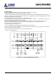
Active non power-
down standby
current
IDD3N
one bank active, CKE is HIGH; CS is HIGH, tCK =
tCKmin; address and control inputs are SWITCHING; data
bus inputs are STABLE
25 20 20 mA
Active non power-
down standby
current with clock
stop
IDD3NS
one bank active, CKE is HIGH;
CS is HIGH, CK = LOW,
CK = HIGH; address and control inputs are
SWITCHING; data bus inputs are STABLE
15 12 12 mA
Operating burst
read current
IDD4R
one bank active; BL = 4; CL = 3; tCK = tCKmin ;
continuous read bursts; IOUT = 0 mA; address inputs are
SWITCHING; 50% data change each burst transfer
75 70 70 mA
Operating burst
write current
IDD4W
one bank active; BL = 4; tCK = tCKmin ; continuous write
bursts; address inputs are SWITCHING; 50% data change
each burst transfer
55 50 50 mA
Auto-Refresh
Current
IDD5
tRC = tRFCmin ; tCK = tCKmin ; burst refresh; CKE is
HIGH; address and control inputs are SWITCHING; data
bus inputs are STABLE
50 50 50 mA
Deep Power-
Down current
IDD8(4)
Address and control inputs are STABLE; data bus inputs
are STABLE
10 10 10 uA
AS4C16M16MD1
256Mb MOBILE DDR SDRAM
Confidential
- 46/56 -
Ver.1.1 Oct.2015