
Datasheet

8. ELECTRICAL CHARACTERISTIC
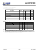
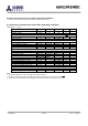
8.1 Absolute Maximum Ratings
PARAMETER SYMBOL
VALUES
UNITS
MIN MAX
Vol
tage on VDD relative to VSS VDD −0.3 2.7 V
Vol
tage on VDDQ relative to VSS VDDQ −0.3 2.7 V
Vol
tage on any pin relative to VSS VIN, VOUT −0.3 2.7 V
O
perating temperature : Tj
-
30
-40
85
85
°C
Storag
e Temperature TSTG −55 150 °C
Short
Circuit Output Current IOUT ±50 mA
Po
wer Dissipation PD 1.0 W
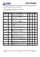
8.2 Input/Output Capacitance
[Notes 1-3]
PARAMETER SYMBOL MIN MAX UNITS NOTES
I
nput capacitance, CK, CK
CCK 1.5 3.0 pF
I
nput capacitance delta, CK, CK
CDCK 0.25 pF
I
nput capacitance, all other input-only pins CI 1.5 3.0 pF
I
nput capacitance delta, all other input-only pins CDI 0.5 pF
I
nput/ output capacitance, DQ,DM,DQS CIO 3.0 5.0 pF 4
I
nput/output capacitance delta, DQ, DM, DQS CDIO 0.50 pF 4
Notes:
1.
These values are guaranteed by design and are tested on a sample base only.
2.
These capacitance values are for single monolithic devices only. Multiple die packages will have parallel capacitive loads.
3.
Although DM is an input-only pin, the input capacitance of this pin must model the input capacitance of the DQ and DQS pins. This is
required to match signal propagat
ion times of DQ, DQS and DM in the system.
AS4C16M16MD1
256Mb MOBILE DDR SDRAM
Confidential
- 44/56 -
Ver.1.1 Oct.2015