
Datasheet


1. GENERAL DESCRIPTION
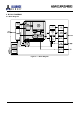
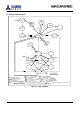
This AS4C16M16MD1 is 268,435,456 bits synchronous double data rate Dynamic RAM. Each 67,108,864 bits bank is organized
as 8,192 rows by 512 columns by 16 bits, fabricated with Alliance Memory's high performance CMOS technology. This device uses a
double data rate architecture to achieve high- speed operation. The double data rate architecture is essentially a 2n-prefetch
architecture with an interface designed to transfer two data words per clock cycle at the I/O balls. Range of operating
frequencies, programmable burst lengths and programmable latencies allow the same device to be useful for a variety of high
bandwidth and high performance memory system applications.
2. FEATURES
•AS4C16M16MD1
• CAS Latency: 2 and 3
VDD/VDDQ = 1.7~1.95V
• Burst Length: 2, 4, 8 and 16
• Data width: x16
• Burst Type: Sequential or Interleave
• Clock rate: 200MHz,166MHz , 133MHz
• 64 ms Refresh period
• Partial Array Self-Refresh(PASR)
• Interface: LVCMOS
• Auto Temperature Compensated Self-Refresh(ATCSR)
• Operating Temperature Range
• Power Down Mode
• Deep Power Down Mode (DPD Mode)
Extended (-30℃ to + 85 ℃)
• Programmable output buffer driver strength
• Four internal banks for concurrent operation
• Data mask (DM) for write data
• Clock Stop capability during idle periods
• Auto Pre-charge option for each burst access
• Double data rate for data output
• Differential clock inputs (CK and CK )
• Bidirectional, data strobe (DQS)
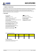
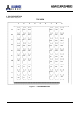
Table 1. Ordering Information
B: indicates BGA package
C: indicates Extended temp
I: indicates Industrial temp (to follow at a later date)
N: Indicates lead free and ROHS compliant
Part Number
Clock
rate
Package
Temperature
Temp Range
AS4C16M16MD1-6BCN
166MHz
60-ball FPBGA
(8.0X9.0 mm)
Extended
-30°C to +85°C
AS4C16M16MD1
256Mb MOBILE DDR SDRAM
Confidential
- 4/56 -
Ver.1.1 Oct.2015