
Datasheet


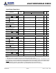


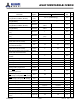

IDD Specification
VDD, VDDQ = 1.35V (1.283V to 1.45V)
Conditions Symbol
IDD max.
Unit
Operating One Bank Active-Precharge Current; CKE: High; External clock:
On; tCK, nRC, nRAS, CL: see timing used table; BL: 8; AL: 0; CS
: High be-
tween ACT and PRE; Command, Address: partially toggling; Data IO: FLOAT-
ING; DM:stable at 0; Bank Activity: Cycling with one bank active at a time;
Output Buffer and RTT: Enabled in Mode Registers; ODT Signal: stable at 0
IDD0
67
mA
Operating One Bank Active-Read-Precharge Current; CKE: High; External
clock: On; tCK, nRC, nRAS, nRCD, CL: see timing used table; BL: 81; AL: 0;
CS
: High between ACT, RD and PRE; Command, Address, Data IO: partially
toggling; DM:stable at 0; Bank Activity: Cycling with one bank active at a time;
Output Buffer and RTT: Enabled in Mode Registers; ODT Signal: stable at 0
IDD1
76
mA
Precharge Power-Down Current Slow Exit; CKE: Low; External clock: On;
tCK, CL: see timing used table; BL: 8; AL: 0; CS
: stable at 1; Command, Ad-
dress: stable at 0; Data IO: FLOATING; DM: stable at 0; Bank Activity: all
banks closed; Output Buffer and RTT: Enabled in Mode Registers; ODT Sig-
nal: stable at 0; Pre-charge Power Down Mode: Slow Exit
IDD2P0
12
mA
Precharge Power-Down Current Fast Exit; CKE: Low; External clock: On;
tCK, CL: see timing used table; BL: 8; AL: 0; CS
: stable at 1; Command, Ad-
dress: stable at 0; Data IO: FLOATING; DM:stable at 0; Bank Activity: all banks
closed; Output Buffer and RTT: Enabled in Mode Registers; ODT Signal: sta-
ble at 0; Pre-charge Power Down Mode: Fast Exit
IDD2P1
20
mA
Precharge Standby Current; CKE: High; External clock: On; tCK, CL: see
timing used table; BL: 8; AL: 0; CS
: stable at 1; Command, Address: partially
toggling; Data IO: FLOATING; DM:stable at 0; Bank Activity: all banks closed;
Output Buffer and RTT: Enabled in Mode Registers; ODT Signal: stable at 0
IDD2N
32
mA
Precharge Quiet Standby Current; CKE: High; External clock: On; tCK, CL:
see timing used table;
BL: 8; AL: 0; CS
: stable at 1; Command, Address: stable at 0; Data IO: FLOAT-
ING; DM: stable at 0; Bank Activity: all banks closed; Output Buffer and RTT:
Enabled in Mode Registers; ODT Signal: stable at 0
IDD2Q
32
mA
Active Power-Down Current; CKE: Low; External clock: On; tCK, CL: see
timing used table; BL: 8; AL: 0; CS
: stable at 1; Command, Address: stable at
0; Data IO: FLOATING; DM: stable at 0; Bank Activity: all banks open; Output
Buffer and RTT: Enabled in Mode Registers; ODT Signal: stable at 0
IDD3P
32
mA
Active Standby Current; CKE: High; External clock: On; tCK, CL: see timing
used table; BL: 8; AL: 0; CS
: stable at 1; Command, Address: partially toggling;
Data IO: FLOATING; DM: stable at 0; Bank Activity: all banks open; Output
Buffer and RTT: Enabled in Mode Registers; ODT Signal: stable at 0
IDD3N
45
mA
AS4C128M16D3LB-12BCN
Confidential
- 31/45 -
Rev.1.0 Mar 2016