
Specification

[AP1034]
016003455-E-01 - 6 - 2016/06
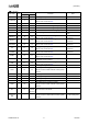
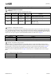
7. Absolute Maximum Ratings
Parameter
Symbol
min
max
Unit
Condition
Motor Power Supply Voltage VM -0.5 35 V
Digital Input/Output Terminal Voltage
(STEP, DIR, RESETB, MODE1,
MODE2, ENABLEB, SLEEPB, FS)
Vterm1 -0.5 5.5 V
VM Level Terminal Voltage
(OUT1A,OUT1B, OUT2A,OUT2B)
Vterm2
-0.5 VM V
VG,CH Terminal Voltage
Vterm3
VM
-0.5
VM
+5.5
V
The Min value must not
exceed -0.5V.
VDC Terminal Voltage
VDC -0.4 5.5 V
V
REF
Input Voltage
VREF
-0.5
VDC
V
CL Terminal Voltage
VCL
-0.5
VDC
V
IS1,IS2 Terminal Voltage
ISn
-0.5
1.5
V
Output Current
Iload
-
2.5
A
(Note 3, Note 4)
Power Dissipation
32QFN PD1
-
3.9
W
Ta=25°C (Note 4, Note 5)
-
2.0
W
Ta=85°C (Note 4, Note 5)
24QFN PD2
-
3.1
W
Ta=25°C (Note 4, Note 5)
-
1.6
W
Ta=85°C (Note 4, Note 5)
Junction Temperature
Tj
-
150
°C
Storage Temperature
Tstg
-40
150
°C
Note 2. All above voltages are with respect to GND. The each power supply of VC and VM is sequence-free.
Note 3. For Power Dissipation, the output current rating may be limited by duty cycle, Ta, and PCB board heat
sinking design.
Note 4. Exposed Pad must be connected to GND.
Note 5. A 4-layer JEDEC51 compliant board is used.
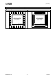
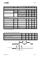
If the temperature exceeds 25°C, be sure to derate at
Figure 2.
24-pin QFN: RθJA =40°C /W
32-pin QFN: RθJA =32°C /W
WARNING: Operation at or beyond these limits may result in permanent damage to the device. Normal
operation is not guaranteed at these extremes.
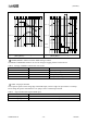
-30 -25 0 25 50 75 85 100 125 150 175
4.5
4.0
3.5
3.0
2.5
2.0
1.5
1.0
0.5
0.0
Temperature (°C)
Power dissipation, Pd ( W)
32QFN
RθJA=32°C/W at 4-layer PCB
24QFN
RθJA=40°C/W at 4-layer PCB
Figure 2. Maximum Power Dissipation