
Specification

[AP1034]
016003455-E-01 - 2 - 2016/06
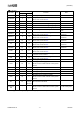
3. Table of Contents
1. General Description ........................................................................................................................................... 1
2. Features .............................................................................................................................................................. 1
3. Table of Contents ............................................................................................................................................... 2
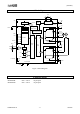
4. Block Diagram ................................................................................................................................................... 3
5. Ordering Guide .................................................................................................................................................. 3
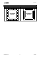
6. Pin Configurations and Function ....................................................................................................................... 4
Pin Configurations ...................................................................................................................................... 4
Functions .................................................................................................................................................... 5
7. Absolute Maximum Ratings .............................................................................................................................. 6
8. Recommended Operating Conditions ................................................................................................................ 7
9. Electrical Characteristics .................................................................................................................................... 7
10. Functional Descriptions ..................................................................................................................................... 9
10.1 Input and Output of Terminal ..................................................................................................................... 9
Truth Table ................................................................................................................................................. 9
ENABLEB : Output Enable Terminal ....................................................................................................... 9
SLEEPB : Sleep Mode Setting Terminal ................................................................................................... 9
MODE1,MODE2 : Motor Excitation Mode Setting Terminal ................................................................. 10
STEP : Step Input Terminal ..................................................................................................................... 10
DIR : Motor Rotation Direction Setting Terminal .................................................................................. 11
RESETB : Home Position Setting Terminal ............................................................................................ 11
FS : PWM Chopper Frequency Select Terminal ...................................................................................... 12
10.2 PWM Constant Current Control ............................................................................................................... 12
Setting of the Output Current ................................................................................................................... 12
Mixed Decay Mode Current Waveform ................................................................................................... 13
Blanking Time .......................................................................................................................................... 13
Output Transistor Operating Mode .......................................................................................................... 13
10.3 Micro-Step Function ................................................................................................................................. 14
Step Sequence .......................................................................................................................................... 14
Example of Current Waveforms in Each Excitation Mode ...................................................................... 15
10.4 Protection Functions ................................................................................................................................. 17
Thermal Shutdown Circuit (TSD) ............................................................................................................ 17
Under Voltage Lock Output Circuit (UVLO) .......................................................................................... 17
Over Current Protection Circuit (OCP) .................................................................................................... 18
11. Recommended External Circuit ....................................................................................................................... 19
Recommended External Circuit ............................................................................................................... 19
Recommended Layout .............................................................................................................................. 20
12. Package ............................................................................................................................................................ 21
Outline Dimensions .................................................................................................................................. 21
Marking .................................................................................................................................................... 23
13. Revise History .................................................................................................................................................. 24
IMPORTANT NOTICE ..................................................................................................................................... 25