
Installation Instructions
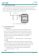

AI-NB25
NB-IoT Module
Sichuan AI-Link Technology Co.,Ltd. page 8 of 20
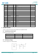
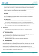
3.3 RF Reference Design
The RF trace in host PCB connected to the module RF antenna pad should be coplanar waveguide
line microstrip line, whose characteristic impedance should be set to 50Ω. It is recommended to use
coplanar waveguide line. The characteristic impedance of coplanar waveguide line could been affected
by many factors, such as dielectric constant, distance between signal layer and reference ground(H), line
width(W), clearance between line and ground(S), copper foil thicknesses(T). The relative relationship
between those parameters could be obtained through software like CITS25, shown as follows.
Fig. 2 Coplanar Waveguide Line Structure (Software Calculation)
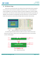
The reference ground would be different for different host PCB. It should set the top layer
As RF trace and set layer2 or bottom layer as reference ground for four-layer or two-layer PCB,
as shown in following figure.
Fig. 3 PCB strack recommend