
Technical data


5-22 Service Guide N5230-90025
Theory of Operation PNA Series Microwave Network Analyzers
Receiver Group Operation N5230C
Receiver Group Operation
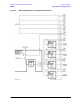
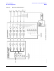
The receiver group measures and processes the input signals into digital information for processing and
eventual display. Figure 5-7 on page 5-23 is a simplified block diagram of the receiver functional group.
In this section the following assemblies are described:
• A20 Mixer Brick
• A5 SPAM Board (Analog Description)
• A29 Reference Channel Switch, Limiter, and DC Block (Options 146 and 246)
A20 Mixer Brick
This assembly contains five identical amplifiers, mixers, and filters. With the spur avoidance function OFF,
the test signals (channels A, B, C, and D) and the reference signal (channel R) are mixed with a synthesized
source signal that is 7.66 MHz higher than the source incident signal to produce a 7.66 MHz IF signal.
With the spur avoidance function ON, at frequencies below 40 MHz, the IF is set to various values between
1 and 12 MHz to avoid spurious responses that could interfere with the measurement. Because of this, the
spur avoidance function should be OFF when troubleshooting the PNA.
The analog IF signal is sent to the A5 SPAM board where it is converted to digital information.
A5 SPAM Board (Analog Description)
The A5 SPAM board contains digital and analog circuitry. For digital descriptions, refer to “A5 SPA M Boar d
(Digital Description)” on page 5-28.
In this assembly, the IF signals from the A, B, C, D, and R mixers go through a gain stage where small signals
are amplified to ensure that they can be detected by the analog-to-digital converter (ADC).
All five signals are sampled simultaneously by the ADCs, where they are converted to digital form. The ADC
conversions are triggered by timing signals from the digital signal processor (DSP) in response to commands
from the central processing unit (CPU). The digitized data is processed into magnitude and phase data by the
DSP and sent to the CPU random access memory (RAM) by way of the peripheral component interconnect
(PCI) bus.
The processed and formatted data is finally routed to the display, and to the general-purpose interface bus
(GPIB) for remote operation. Refer to “Digital Processing and Digital Control Group Operation” on page 5-25 for
more information on signal processing.
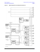
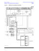
A29 Reference Channel Switch, Limiter, and DC Block (Options 146 and 246)
In these assemblies, the reference signals from the A19 source 1 MASSQuad and the A18 source 2
MASSQuad are switched into the reference receiver mixer in the A20 mixer brick. See Figure 5-8 on page 5-24.
The reference signal comes from the synthesized source, passes through the A29 reference channel switch,
goes through the limiter and DC block, through a front-panel jumper, and then to the receiver reference input of
the A20 mixer brick.
The limiter and DC block protect the A29 reference channel switch from possible damage caused by signals
that may be input into the front-panel Reference SOURCE OUT connector.