
User`s guide
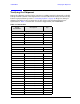
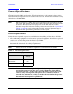
Table Of Contents
- U3042AE12
- Title Page
- TOC
- Introduction
- Description
- Available Options
- Verifying the Shipment
- General Specifications
- Typical Reflection Tracking
- Front and Rear Panel Features
- System Setup with N5230A/C
- Controlling the Test Set with N5230A
- System Setup with N5242A
- Controlling the Test Set with N5242A or N5230C
- DUT Control Lines
- Test Set I/O Interface Commands
- Operational Check
- Troubleshooting Operational Check Failures
- Service Information
- Theory of Operation
- RF Switch Components
- S100 - Source to Ports (1, 5, 9 and 13)
- S200 - Source to Ports (2, 6, 10 and 14)
- S300 - Source to Ports (3, 7, 11 and 15)
- S400 - Source to Ports (4, 8, 12 and 16)
- S101 - Receiver to Ports (1, 5, 9 and 13)
- S201 - Receiver to Ports (2, 6, 10 and 14)
- S301 - Receiver to Ports (3, 7, 11 and 15)
- S401 - Receiver to Ports (4, 8, 12 and 16)
- RF Coupler Components
- System Block Diagram
- Safety and Regulatory Information
- Electrostatic Discharge Protection
- Contacting Agilent
User’s Guide 9
U3042AE12 General Specifications
Frequency Range and Maximum Power Levels
CAUTION It is recommend that you do not operate components near damage levels
(+30 dBm). The power levels must be 3 dB below maximum level to ensure no
damage. See Table 7.
NOTE Refer to your PNA specifications to determine the maximum input power
levels for the PNA access and test ports, or to optimize the power levels in the
receivers.
NOTE Damage and maximum levels are not necessarily the optimum level.
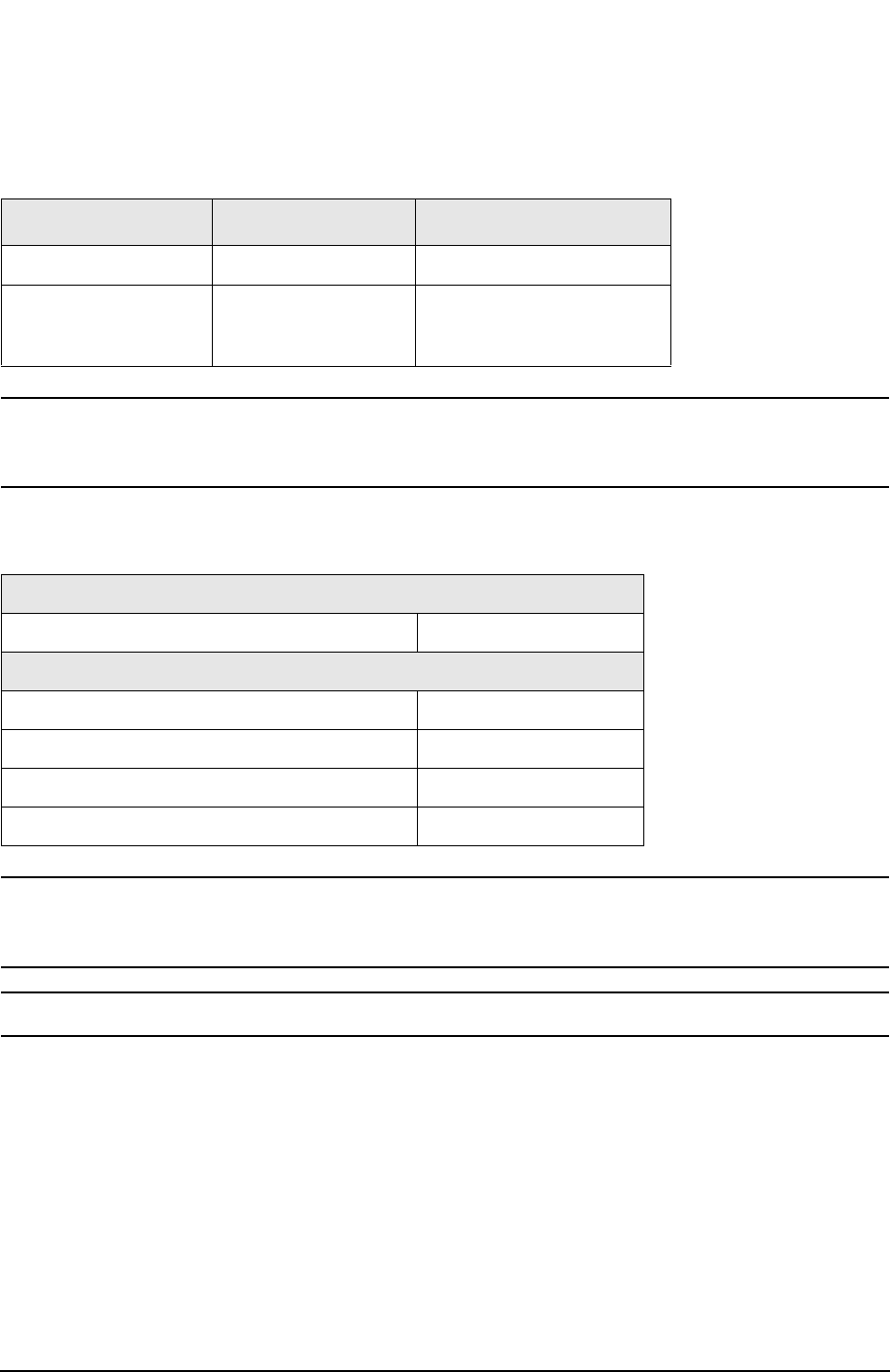
Table 6 Usable Frequency Range
Model Standard 001 or 002
N5230A/C (PNA-L)
10 MHz to 20 GHz 10 MHz to 20 GHz
N5242A (PNA-X)
10 MHz to 26.5 GHz 10 MHz to 26.5 GHz
(significantly degraded
performance above 20 GHz)
Table 7 Power Levels
Maximum U3042AE12 Test Port RF Power Levels:
PORT 5-16 +27 dBm 0 Vdc
Maximum U3042AE12 Access Ports:
SOURCE OUT +20 dBm 0 Vdc
CPLR ARM +20 dbm 0 Vdc
CPLR THRU +20 dBm 0 Vdc
RCVR OUT +20 dBm 0 Vdc