
User guide
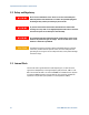
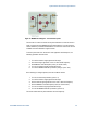
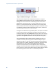
Table Of Contents
- 1 Getting Started
- 2 N4962A System Overview
- 3 System Details and Performance Specifications
- 4 Operation
- 5 Remote GPIB Interface
- 6 Returning the N4962A Serial BERT to Agilent Technologies

N4962A System Overview
Serial BERT 12.5 Gb/s User Guide 21
2.2 Rear Panel Quick Reference
Figure 4. N4962A rear panel
Connectors
DataThru
¯¯¯¯¯¯ , DataThru (SMA) – connected to IN¯¯, IN when ‘thru’ data path
selected.
PatTrigO (SMA)
– PRBS pattern trigger output
TX CKI (SMA)
– PRBS generator clock input (default connected to TX CKO)
RX CKI (SMA)
– error detector clock input (default connected to RX CKO)
RX CKO (SMA)
– internal clock output for error detector
TX CKO (SMA)
– internal clock output for PRBS generator
HF TrigO (SMA)
– high-frequency (9.85 – 11.35 GHz) clock output
LF TrigO (SMA)
– low-frequency (616 – 709 MHz) clock output
Ext CKI (SMA)
– low-frequency (616 – 709 MHz) clock input; used to phase
lock with external clock source
JitterI (SMA)
– jitter signal input (DC-100 MHz); turn jitter mode on before use
(GPIB)
– GPIB connector, conforms to IEEE 488.1 mechanical specification
Label
SN (white area)
– N4962A serial number
Controls
GPIB (switch panel)
– N4962A GPIB address (down is ‘0’, up is ‘1’, LSB is on
the left)
(Default GPIB address as shipped from the factory is 25)
Power (switch)
– N4962A is powered when switch is toggled up towards
‘Power’ label
Power connector
– connects with AC/DC adapter. Use only the supplied
AC/DC adapter.