Agilent HDMP-3001 Ethernet over SONET Mapper IC Device Specification Data Sheet Table of Contents 1. Introduction ............................................................................................... 5 1.1 Internal Functional Blocks .............................................................. 5 1.2 HDMP-3001 Features List ................................................................ 5 1.3 Applications .......................................................................................
3.9 SONET/SDH Processing ................................................................. 24 3.9.1 Transmit SONET/SDH Processing Overview ...................... 24 3.9.2 Receive SONET/SDH Processing Overview ........................ 25 3.9.3 Transmit SONET/SDH Processing Details ........................... 25 3.9.4 Receive SONET/SDH Processing Details ............................. 30 4. Application Information ........................................................................ 38 4.
List of Figures Figure 1. Functional Block Diagram ......................................................... 5 Figure 2. HDMP-3001 applications ............................................................ 6 Figure 3. HDMP-3001 pin assignments ..................................................... 7 Figure 4. GFP Payload Bit Order ............................................................. 18 Figure 5. GFP FCS Bit Order .................................................................... 18 Figure 6.
List of Tables Table 1. Line Side Interface Pins Description ........................................... 8 Table 2. MII Interface Pins Description ..................................................... 9 Table 3. Transport Overhead Pins Description ...................................... 10 Table 4. Microprocessor Interface Pins Description ............................. 12 Table 5. JTAG Interface Pins Description ............................................... 13 Table 6.
1. Introduction The Agilent HDMP-3001 is a highly integrated VLSI device that provides mapping of Ethernet encapsulated packets into STS-3c payloads. The HDMP-3001 supports full-duplex processing of SONET/SDH data streams with full section, line, and path overhead processing. The device supports framing pattern, scrambling/descrambling, alarm signal insertion/detection, and bit interleaved parity (B1/B2/B3) processing. Serial interfaces for SONET/SDH TOH overhead bytes are also provided.
• Implemented in 0.25 micron CMOS with 1.8 V core, 3.3 V I/O power and LVCMOS compatible I/Os. • Provides a 16-bit general purpose I/O (GPIO) register. • Device power-up initialization optionally through 2-wire EEPROM interface. • Configurable by hardware to be connected to either a PHY or a MAC from the system connectivity viewpoint. 1.3 Applications • Multi-Service Ethernet Switches. • Enhanced Services SONET/ SDH Add/Drop Multiplexers (ADMs). • DSU/CSUs. 1.
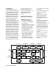
2. Pinout 125 130 135 140 115 10 110 15 105 20 100 25 95 30 90 35 75 70 65 60 DVDD CPU_CLK GND VDD ADDR[3] ADDR[4] ADDR[5] ADDR[6] ADDR[7] ADDR[8] D[0] DGND GND D[1] D[2] D[3] D[4] D[5] D[6] D[7] DVDD DGND 55 50 DGND VDD GPIO[15] RDYB WRB RDB ADDR[0] ADDR[1] ADDR[2] 45 85 Figure 3.
2.2 Pin Descriptions Table 1. Line Side Interface Pins Description Signal name Pin # Type(I/O) Signal description RX_DATA[0] RX_DATA[1] RX_DATA[2] RX_DATA[3] RX_DATA[4] RX_DATA[5] RX_DATA[6] RX_DATA[7] 25 26 27 28 29 32 33 34 I RECEIVE DATA: Byte-wide STS-3c data input stream. RX_DATA [7] is the MSB, and RX_DATA [0] the LSB. Data is sampled on the rising edge of RX_SONETCLK.
Signal name Pin # Type(I/O) Signal description TX_FRAME_SFP 125 O TRANSMIT FRAME POSITION OUTPUT INDICATOR: Frame position indication signal is active high and indicates the SONET frame position on the TX_DATA [7:0] bus. Updated on the rising edge of TX_SONETCLK. This signal is also used for the outer board to start sending the first bit (MSB) of the serial data E1, E2, F1, SDCC, and LDCC.
Signal name Pin # Type(I/O) Signal description MDIO 113 I/O MII management input/output serial data. When this interface is unused, connect this pin high. If HDMP-3001 is attached to a MAC via the mechanical interface specified in IEEE 802.3, clause 22.6, an external pull-up of 1.5 kohm ± 5% is required. MDC 114 I MII management clock, up to 2.5 MHz. When this interface is unused, connect this pin high. Table 3.
Signal name Pin # Type(I/O) Signal description TX_E1_DATA 126 I TRANSMIT E1 DATA: Local orderwire channel data byte (E1) to be inserted by the HDMP-3001 into the outgoing SONET data stream. TX_E2_DATA 127 I TRANSMIT E2 DATA: Express orderwire channel data byte (E2) to be inserted by the HDMP-3001 into the outgoing SONET data stream. TX_F1_DATA 128 I TRANSMIT F1 DATA: Maintenance channel data byte (F1) to be inserted by the HDMP-3001 into the outgoing SONET data stream.
Table 4. Microprocessor Interface Pins Description Signal name Pin # Type(I/O) Signal description ADDR[0] ADDR[1] ADDR[2] ADDR[3] ADDR[4] ADDR[5] ADDR[6] ADDR[7] ADDR[8] 56 57 58 63 64 65 66 67 68 I ADDRESS BUS: Allows host microprocessor to perform register selection within the HDMP-3001. APS_INTB 83 O (O/D) APS INTERRUPT: Active-low output triggered by an APS event. APS_INTB is an open-drain output which is in a high impedance state when inactive. When used, this pin needs an external pull-up.
Signal name Pin # Type(I/O) Signal description INT 86 O (T/S) INTERRUPT: Configurable interrupt output. Refer to Table 18 for a detailed description of how INT is configured. In open-drain configurations, an external pull-up is required. In open-source configurations, an external pull-down is required. To prevent undesired interrupts before configuration is complete, microprocessors with an active-high interrupt pin should have a pull-down and those with an active-low interrupt pin, a pull-up.
Table 6. Two-Wire EEPROM Interface Pins Description Signal name Pin # Type(I/O) Signal description SCL 92 I/O EEPROM bus clock. If no EEPROM is present, connect this pin to ground. Refer to EEPROM application notes for board pull-up requirements. SDA 89 I/O EEPROM bus data. If no EEPROM is present, connect this pin to ground. Refer to EEPROM app notes for board pull-up requirements. Table 7.
Signal name Pin # Type(I/O) Signal description DGND 10, 11, 20, 40, 50, 70, 80, 90, 100, 110, 120, 130, 140, 150, 160 Driver GROUND: These pins should be connected to the I/O ground plane. VDD 2, 22, 42, 51, 62, 82, 91, 102, 122, 131, 142 Logic POWER: These pins should be connected to the 1.8 V power supply for logic. DVDD 19, 39, 59, 79, 99, 119, 139, 159 Driver POWER: These pins should be connected to the 3.3 V power supply for I/O.
2.3 I/O Buffer Types This section lists the types of some particular I/Os used in the HDMP-3001 chip. Table 8.
3. Functional Description 3.1 Introduction The HDMP-3001 performs fullduplex mapping of Ethernet frames into a SONET STS-3c / SDH STM-1 payload using the LAPS or GFP protocol. All SONET/SDH framing functions are included. A TOH interface provides direct add/drop capability for E1, E2, F1, and both Section and Line DCC channels. SONET or SDH mode is selected during initial configuration. By default, the HDMP-3001 operates in LAPS mode. LAPS is a HDLC-compatible protocol.
3.2.5 SONET/SDH Interface This interface is 8 bits wide and runs at 19.44 MHz. The Serial SONET/SDH overhead channels are clocked in and out of the IC through low-speed serial ports. 3.3 Initialization 3.3.1 Hardware reset The HDMP-3001 hardware reset, RSTB, is asynchronous and must be active for at least 200 SONET clock cycles (>10 µs) with stable power. 3.3.2 Software Reset Software resets are functionally equivalent to hardware resets.
3.4.2 LAPS Mode In LAPS mode the FCS is calculated LSB first and the FCS sum is transmitted in reversed bit order within each byte. See Figure 6 and Figure 7. 3.5 Performance Monitoring For performance monitoring purposes, the HDMP-3001 contains a number of delta bits, event bits and error counters. Delta bits are set by the HDMP3001 when a monitored parameter changes state. The delta bit then stays high until the controller clears the bit.
Summary delta event bits provide a consolidated view of the various individual delta event bits, grouped either by function or SONET tributary. Summary delta events are therefore a function of the other delta events bits in the register maps. The summary bits are read only, and will only be cleared when all delta event bits that contribute to them are cleared. The summary bits are O/R'd together to form the HDMP-3001 interrupt outputs, INTB and APS_INTB.
3.6.2 JTAG The HDMP-3001 supports the IEEE 1149.1 Boundary Scan standard. The Test Access Port consists of 5 pins as defined in Table 10. Signals TDI, TMS and TRSTSB are all pulled up to logic one when not driven. Table 9.
EOS_D_SUM group indicates that at least one of the delta signals below is unmasked and set.
packet. When this occurs an interrupt is generated. The packet can be ended via generation of an FCS error, via an abort sequence, or via “fill” bytes inserted in the gap, depending upon a software configurable escape code. • Maintains performance monitor counters. 3.8.1.1 FCS Polynomial for LAPS Processing The HDMP-3001 supports CRC-32 Frame Check Sequence (FCS) generation and checking.
PLI '+' 0xB6 NUMBER OF BYTES IN THE GFP PAYLOAD LSB PLI '+' 0xAB MSB cHEC '+' 0x31 LSB cHEC '+' 0xE0 MSB TYPE PROGRAMMABLE LSB TYPE PROGRAMMABLE MSB tHEC LSB tHEC MAC PAYLOAD 64-1522 BYTES MSB LSB FCS[31:24] 1) 32-BIT CRC POLYNOMIAL FCS[23:16] 2) ON PRE-SCRAMBLED DATA FCS[15:8] 3) COVERS THE GFP PAYLOAD DATA ONLY FCS[7:0] BIT TRANSMISSION ORDER Figure 11. The GFP frame 3.8.2.
• Line/MS REI, M1 • Transmits undefined TOH/SOH as fixed all zeros. • Scrambles payload using SONET/SDH frame synchronous descrambler, polynomial (X7 + X6 +1). 3.9.2 Receive SONET/SDH Processing Overview The Receive SONET/SDH Processor provides for the framing of the STS signal, descrambling, TOH/ SOH monitoring including B1 and B2 monitoring, AIS detection, pointer processing, and POH monitoring.
3.9.3.2 POH There are nine bytes of path overhead. The first byte of the path overhead is the path trace byte, J1. Its location with respect to the SONET/SDH TOH/SOH is indicated by the associated STS/AU pointer. The following sections define the transmitted values of the POH bytes. Where the byte names differ between SONET and SDH, the SONET name is listed first. 3.9.3.2.1 Path Trace (J1) The HDMP-3001 can be programmed to transmit either a 16-byte or a 64-byte path trace message in the J1 byte.
Table 11. Path RDI bit values PRDI_AUTO PRDI_ENH RX_PAIS RX_LOP RX_UNEQ RX_PLM G1 Bits 5, 6, and 7 0 x x x x TX_G1[2:0] 1 0 1 x x 100 0 x x 000 1 x x 101 0 1 x 110 0 0 1 010 0 0 0 001 1 3.9.3.2.9 POH AIS Generation Normal generation of SONET/ SDH payload is suspended during transmission of the Line (Multiplex Section or MS) Alarm Indication Signal, LAIS, or the Path (Administrative Unit or AU) AIS signals, PAIS. AIS is generated if: • TX_LAIS or TX_PAIS = 1.
Table 12. STS-3c/STM-1 TOH/SOH Row Column 1 2-3 4 5-6 7 8-9 1 A1[1] A1[2,3] A2[1] A2[2,3] J0[1] Z0[2,3] 2 B1 E1 F1 3 D1 D2 D3 4 H1[1] H1[2,3] H2[1] 5 B2[1] B2[2,3] K1 K2 6 D4 D5 D6 7 D7 D8 D9 8 D10 D11 D12 9 S1 1 Z1[2,3] Z2[1] 1 H2[2,3] 1 Z2[2] , M1 H3[1] H3[2,3] E2 Note: 1. The Z1 and Z2 bytes are nonstandardized reserved bytes for STM-1. 3.9.3.3.4 Section Growth/Spare (ZO) Section Trace The Z0 bytes are transmitted in order as 2 and 3.
Non-AIS Generation. The first H1-H2 byte pair is transmitted as a normal pointer with: • NDF = 0110 • SS (SONET/SDH) = 0 • Pointer Value = 10_0000_1010 All other H1-H2 byte pairs are transmitted as concatenation indication bytes, with • NDF =1001 • SS = 0 • Pointer Value = 11_1111_1111. See Figure 14. 3.9.3.3.9 Line/MS BIP-24 (B2) There are three B2 bytes in the TOH/SOH, and together they provide a BIP-24 error detection capability.
scrambles the entire SONET/SDH frame except for the first row of TOH/SOH. For testing purposes, the scrambler can be disabled through the SCR_INH bit in the register map. sistent frame value is received, it is written to RX_J0[15:0]_[7:0]. The first byte of the section trace frame (which contains the frame start marker) is written to RX_J0[15]_[7:0]. 3.9.4 Receive SONET/SDH Processing Details 3.9.4.
3.9.4.2.9 APS Monitoring If the K1 byte and the four MSBs of the K2 byte, which are used to send APS requests and channel numbers, are received identically for three consecutive frames, their values are written to RX_K1[7:0] and RX_K2[7:4]. Accepted values are compared to the previous contents of these registers, and when a new 12-bit value is stored, the RX_K1_D delta bit is set. The K1 byte is checked for instability.
• If PTR_STATE[1:0] = 00 and {LOP2,AIS2} = 11 and {LOP3,AIS3} = 11, which is the normal case, then RX_PAIS = 0 and RX_LOP = 0. • If PTR_STATE[1:0] = 01 and {LOP2,AIS2} = 01 and {LOP3,AIS3} = 01, then RX_PAIS = 1 and RX_LOP = 0. • If PTR_STATE[1:0] = 10 and {LOP2,AIS2} = 01 and {LOP3,AIS3} = 10, then RX_PAIS = 0 and RX_LOP = 1. The RX_PAIS and RX_LOP signals contribute to the Path Remote Defect Indication (PRDI). Changes in these state values are indicated by the RX_PAIS_D and RX_LOP_D delta bits. 3.9.4.
cates that the VC-4 starts three bytes after the K2 byte. In addition, 8-bit counters are provided for counting positive and negative justification events, as well as NDF events. Status bits are provided for indicating the detection of negative justification, positive justification, NDF, invalid pointer, new pointer and concatenation indication. When the LOP or LOPC states are entered as indicated in Figures 15 and 16, the LOP interrupt request bit in the corresponding OR#IRQ2 register will be set.
Table 13. Pointer Processing Norm_point: Normal NDF AND match of ss bits AND offset value in range. NDF_enable: NDF enabled AND match of ss bits AND offset value in range. AIS_ind: 11111111 11111111. Incr_ind: Normal NDF AND match of ss bits AND majority of I bits inverted AND no majority of D bits inverted AND previous NDF_enable, incr_ind or decr_ind more than three frames ago.
can result in from 0 to 8 mismatches (B3 bit errors). This value can be inserted into the Transmit Side G1 byte from bit one to bit four as a Path REI. The HDMP-3001 contains a 16-bit B3 error counter that counts every B3 bit error. When the performance monitoring counters are latched (LATCH_EVENT transitions high), the value of this counter is latched to the B3ERRCNT[15:0] register, and the B3 error counter is cleared. 3.9.4.9.
high-speed device that locates frame, does byte de-interleaving, and performs serial-to-parallel conversion of an STS-3c/STM-1 signal. 3.9.4.11 Framer Enabled Details If the framer is enabled (RX_FRMR_INH = 0), the HDMP-3001 device performs the framer processing as follows. When the framer state machine is out-of-frame (RX_OOF = 1), it searches for the 32-bit A1-A1-A2A2 framing byte sequence of 0xF6F6_2828. This pattern may start on any of the 8 input data lines and span up to five input bytes.
3.9.4.14 B1 Monitor In both modes, the HDMP-3001 checks the received B1 bytes for correct Bit Interleaved Parity 8 (BIP-8) values. Even parity BIP-8 is calculated over all bytes of each frame before descrambling. This value is then compared to the received B1 value in the following frame after descrambling. The comparison can result in 0 to 8 mismatches (B1 bit errors). The HDMP-3001 contains a 16-bit B1 error counter that counts every B1 bit error.
4. Application Information 4.1 Chip setup and configuration 4.1.1 EEPROM Detection After reset, HDMP-3001 will probe the SDA pin. If tied to ground, no boot EEPROM is present and normal operation will resume. If connected to an EEPROM, SDA is pulled high by an internal resistor and HDMP-3001 will start to load its configuration from the EEPROM. During this time, HDMP-3001 will not respond to any transactions on the microprocessor or MII Management ports. 4.2 Configurations 4.2.
Table 15. INT Pin Configuration Interrupt Mode[1:0] Output Configured Type Int Active Level Description 00 (Default) Open-Drain (O/D) 0 Interrupt output INT is asserted with 0 and de-asserted with Z externally. An external resistive pull-up is needed. Output buffer OEN is driven by an inversion of the internally maskable active-high interrupt signal. Output buffer’s input pin is driven to 0. An internally maskable interrupt active value of 1 causes an external interrupt active value of 0.
4.3 Firmware and System Design Information 4.3.1 Board level pull-ups and pull-downs Many of the HDMP-3001 input and tristateable outputs have internal pull-ups. Refer to the pin description for detailed information on where external pull-ups are required. 4.3.2 Motorola MPC860 Microprocessor Interface The recommended setup of the interface is: • OR[20-31] = 000100001000, which sets normal CS timing, no burst allowed, externally generated TA. • HDMP-3001 mapped to the smallest memory bank, 32 Kbytes.
4.3.3 MII Interface 4.3.4 EEPROM Interface Table 17. Pin Connections – MII Interface 4.3.4.1 Configuration 1 HDMP-3001 is set up through the microprocessor or MII Management ports. No EEPROM needed. Connect SCL and SDA to ground. Disable SCL and SDA pull-ups to save power.
5. Register Definitions The HDMP-3001 contains two register maps. One is the MII Management (MDIO) register map, which can only be accessed through the MDIO port. The other register map is the chip register map which can be accessed through the MDIO, microprocessor and EEPROM ports. 5.1 MII Management Register Map The MII Management register map, Table 21, is only accessible through the MII Management port. It is defined in the IEEE 802.
Address Bit Type Bit Name Default value Description 8 R Extended Status Fixed 0 No extended status information in register 15. 7 R Reserved Fixed 0 6 R MF Preamble Suppression Fixed 0 PHY does not allow preamble to be suppressed in management frames. 5 R Auto-Negotiation Complete Fixed 0 Not supported. 4 R Remote Fault Fixed 0 Not supported. 3 R Auto-Negotiation Ability Fixed 0 Cannot auto-negotiate. 2 R Link Status 0 Reflects the SONET status.
5.2 Chip Register Map The chip register map, Table 19, can be accessed through the MDIO, microprocessor and EEPROM interfaces. Table 19.
Address Register Name SONET/SDH Transmit Registers 0x0B4 Transmit G1 Control 0x0B5 Reserved 0x0B6-0x0F5 Transmit J1 Bytes (64) 0x0F6 Reserved 0x0F7 POH Error Generation 0x0F8 Transmit C2 Byte SONET/SDH Receive Registers 0x0F9 Receive LOH Monitor Delta 0x0FA Receive SOH Monitor Delta 0x0FB Reserved 0x0FC Receive LOH Monitor Masks 0x0FD Receive SOH Monitor Masks 0x0FE Reserved 0x0FF Receive TOH Monitor Control 1 0x100 Reserved 0x101 Receive Framer Position Control 0x102 Receiv
Address Register Name 0x122 Receive Pointer Interpreter Mask 0x123-0x125 Reserved 0x126 Receive Pointer Interpreter Delta 0x127 Reserved 0x128 Receive Pointer Status (1) 0x129 Reserved 0x12A Receive Pointer Status (2) 0x12B-0x12C Reserved 0x12D Receive J1 Reading Control 0x12E Receive J1 Mode Control 0x12F Receive RDI Monitor 0x130 Receive J1 Delta 0x131 Receive J1 Mask 0x132 Receive POH Mask 0x133 Receive J1 OOF 0x134-0x173 Receive J1 Bytes (64) 0x174 Receive Path Delta
Address Register Name 0x182 Transmit Control/Type_L Field 0x183 Transmit Rate Adaptation/Type_H Field 0x184-0x185 Transmit FIFO Threshold 0x186 Transmit LAPS mode 0x187 GFP Mode 0x188 TX SAPI LSB / Spare Byte 0x189 TX_SAPI_MSB 0x18A-0x18B Reserved 0x18C-0x18F Transmit MII Frames Received OK Counter 0x190-0x193 Transmit MII Alignment Error Counter 0x194-0x197 TX_ER Error Counter 0x198-0x19B Transmit FIFO Overflow Error 0x19C-0x19F Transmit FIFO Underrun Error 0x1A0 Ethernet Trans
Address Register Name 0x1CF Receive Spare Field Byte 0x1D0 Receive Pre-Sync States 0x1D1-0x1D2 Receive SAPI Field 0x1D3 Reserved 0x1D4-0x1D7 Receive MII Frames Transmitted OK 0x1D8-0x1DB Receive FCS and HEC Error Counter 0x1DC-0x1DF Receive Format and Destination Error Counter 0x1E0-0x1E3 Receive Out of Sync Error Counter 0x1E4-0x1E7 Receive FIFO Overflow Error 0x1E8-0x1EB Receive FIFO Underrun Error 0x1EC Ethernet Receive Interrupt Event 0x1ED Ethernet Receive Interrupt Mask 0x1EF
5.2.1 Common Registers ADDR=0x000: Reset and Performance Latch Control Bit 7 Bit 6 Bit 5 Bit 4 Bit 3 Bit 2 Bit 1 Bit 0 Bit name Reserved Reserved Reserved Reserved LATCH_ CNT Reserved STATE_ RESET GLOBAL_ RESET R/W — — — — R/W — R/W WSR Value after reset 0 0 0 0 0 0 0 0 Bits 7-4: Reserved Bit 3: LATCH_CNT is set to transfer performance monitor counters to registers to read the counter values.
ADDR = 0x003: Microprocessor Interrupt Pin Mode[1:0] Bit 7 Bit 6 Bit 5 Bit 4 Bit 3 Bit 2 Bit 1 Bit name Reserved Reserved SDA_PU_ DIS SCL_PU_ DIS Reserved Reserved INT_MODE[1:0] R/W — — R/W R/W — — R/W Value after reset 0 0 0 0 0 0 2'b00 Bit 0 Bits 7-6: Reserved Bit 5: Bit 4: SDA_PU_DIS disables the internal SDA pull-up when high. SCL_PU_DIS disables the internal SCL pull-up when high.
ADDR = 0x005: PHY Address[4:0] Bit 7 Bit 6 Bit 5 Bit 4 Bit 3 Bit name Reserved Reserved Reserved PHY_ADDR[4:0] R/W — — — R/W Value after reset 0 0 0 0x1B Bit 2 Bit 1 Bit 0 Bits 7-5: Reserved Bits 4-0: PHY_ADDR specifies the PHY address for the HDMP-3001 chip. The chip uses the PHY address to respond to the Management Entity when addressed through the MDIO port.
ADDR=0x007: Event Summary Bit 7 Bit 6 Bit 5 Bit 4 Bit 3 Bit 2 Bit 1 Bit 0 Bit name TOH_D_SUM Reserved PTR_D_SUM POH_D_SUM Reserved EOS_D_SUM Reserved Reserved R/W R — R R R R — — Value after reset 0 0 0 0 0 0 0 0 Bit 7: TOH_D_SUM is set to indicate at least one of the TOH/SOH delta bits (RX_LOS_D, RX_OOF_D, RX_LOF_D, RX_LAIS_D, RX_LRDI_D, J0_OOF_D) is set and its corresponding mask bit is cleared.
ADDR=0x009: Mode of Operation Bit 7 Bit 6 Bit 5 Bit 4 Bit 3 Bit 2 Bit 1 Bit 0 Bit name Reserved Reserved Reserved Reserved ISOLATE_ MII SONET/SDH PHY/MAC GFP/LAPS R/W — — — — R/W R/W R/W R/W Value after reset 0 0 0 0 1 0 0 0 Note that this register only should be programmed when STATE_RESET is active. Bits 7-4: Reserved Bit 3: Bit 2: ISOLATE_MII is set to isolate the HDMP-3001 chip on the MII bus.
ADDR=0x00B: SONET/SDH Configuration Bit 7 Bit 6 Bit 5 Bit 4 Bit 3 Bit 2 Bit 1 Bit 0 Bit name Reserved Reserved TX_UNEQ Reserved Reserved TX_SONET RX_SONET_DSCR Reserved _SCR_INH _INH R/W — — R/W — — R/W R/W — Value after reset 0 0 0 0 0 0 0 0 Bits 7-6: Reserved Bit 5: TX_UNEQ is set to generate all zeros in its SPE/VC bytes to create unequipped SPE. Bits 4-3: Reserved Bit 2: TX_SONET_SCR_INH is set to disable the HDMP-3001 SONET scrambler.
ADDR=0x00E: GPIO [7:0] Data Bit 7 Bit 6 Bit 5 Bit 4 Bit 3 Bit 2 Bit 1 Bit 0 Bit name GPIO7 GPIO6 GPIO5 GPIO4 GPIO3 GPIO2 GPIO1 GPIO0 R/W R/W R/W R/W R/W R/W R/W R/W R/W Value after reset 1 1 1 1 1 1 1 1 Bits 7-0: GPIO[7:0] : General purpose I/O bits 7:0, and they are defaulted as inputs.
5.3 SONET/SDH Transmit Registers ADDR=0x09C: Transmit BIP control Bit 7 Bit 6 Bit 5 Bit 4 Bit 3 Bit 2 Bit 1 Bit 0 Bit name Reserved Reserved Reserved Reserved Reserved TX_B1_INV TX_B2_INV TX_B3_INV R/W — — — — — R/W R/W R/W Value after reset 0 0 0 0 0 0 0 0 This is a BIP calculating control register. Bits 7-3: Reserved Bit 2: Bit 1: TX_B1_INV is set to calculate B1 by odd parity (for testing purposes). TX_B2_INV is set to calculate B2 by odd parity (for testing purposes).
ADDR=0x09F –0x0AE: Transmit J0 Bytes 1 – 16 Bit 7 Bit 6 Bit 5 Bit 4 Bit 3 Bit 2 Bit 1 Bit 0 0 0 0 0 0 0 0 Bit name TX_J0[0]_[7:0] • • • TX_J0[15]_[7:0] R/W R/W Value after reset 0 Bits 7-0: TX_J0[0:15]_[7:0]: Transmit J0 (Section Trace) – When enable, the HDMP-3001 will continuously transmit in the 16-byte pattern in these registers in the J0 byte. The bytes are transmitted in descending order starting from TX_J0[15]_[7:0].
ADDR=0x0B1: Transmit K1 Byte Bit 7 Bit name TEST_K1[7:0] R/W R/W Value after reset 0 Bit 6 Bit 5 Bit 4 Bit 3 Bit 2 Bit 1 Bit 0 0 0 0 0 0 0 0 TX_K1[7:0]: These bits are automatic protection switching (APS) signaling. The HDMP-3001 inserts TX_K1[7:0] into the transmitted K1 byte, and TX_K2[7:3] into the five MSBs of the transmitted K2 byte. The three LSBs are controlled according to the description above (ADDR=0x0b0).
Table 20. G1 values PRDI_ AUTO PRDI_ ENH RX_PAIS || RX_LOP RX_UNEQ RX_PLM G1 Bits 5, 6, & 7 0 x x x x TX_G1[2:0] 1 0 1 x x 100 0 x x 000 1 x x 101 0 1 x 110 0 0 1 010 0 0 0 001 1 ADDR=0x0B6 – 0x0F5: Transmit J1 Bytes 1 – 64 Bit 7 Bit 6 Bit 5 Bit 4 Bit 3 Bit 2 Bit 1 Bit 0 0 0 0 0 0 0 0 Bit name TX_J1[0]_[7:0] • • • TX_J1[63]_[7:0] R/W R/W Value after reset 0 When Transmit J1 (Path Trace) enabled, 1.
ADDR=0x0F7: POH Error Generation Bit 7 Bit 6 Bit name Reserved R/W Value after reset Bit 7: Bit 5 Bit 3 Bit 2 Bit 1 Bit 0 TX_G1 [2:0] Reserved Reserved Reserved TX_PAIS — R/W — — — R/W 0 0 0 0 0 0 0 Bit 4 0 Reserved Bits 6-4: TX_G1[2:0] When PRDI_AUTO = 0, the values transmitted in bits 7-5 of G1 are taken from these three bits.
5.
ADDR=0x0FC: Receive LOH Monitor Masks Bit 7 Bit 6 Bit 5 Bit 4 Bit 3 Bit 2 Bit 1 Bit 0 Bit name J0_OOF_ D_MASK Reserved RX_LAIS_ D_MASK RX_LRDI_ D_MASK RX_K1_D _MASK K1_UNSTAB _D_MASK RX_K2_D _MASK Reserved R/W R/W — R/W R/W R/W R/W R/W — Value reset 1 1 1 1 1 1 1 1 Bit 7: J0_OOF_D_MASK – J0_OOF delta bit mask Bit 6: Bit 5: Reserved, always write as one.
ADDR=0x0FF: Receive TOH Monitor Control Bit 7 Bit 6 Bit 5 Bit 4 Bit 3 Bit 2 Bit 1 Bit 0 Bit name K2_CONSEC_NUM[3:0] RX_LOS_ LEVEL RX_LOS_ INH RX_FRAM_ INH RX_LOF_ ALG R/W R/W R/W R/W R/W R/W Value after reset 0 0 0 0 0 1 0 1 Bits 7-4: K2_CONSEC_NUM[3:0]: This 4 bit register is used to keep track of the number of consecutive occurrences of LAIS and LRDI in order for the presence/absence of LAIS or LRDI to be detected and the monitors to be updated accordingly.
Table 21.
Bit 0: J0_OOF: J0_OOF = 0 when the most significant bits of all J0 bytes are zero except for the MSB of the frame start marker byte. The J0 monitor framer searches for 15 consecutive J0 bytes that have a zero in their MSB and followed by a J0 byte with a zero in its MSB. J0_OOF = 1 once the J0 monitor framer is in frame. It remains in frame until three consecutive J0 bytes are received with at least one MSB bit error.
ADDR=0x104 –0x113: Receive J0 Bytes 0 – 15 Bit 7 Bit 6 Bit 5 Bit 4 Bit 3 Bit 2 Bit 1 Bit 0 Bit name RX_J0 [0]_[7:0] • • • RX_J0 [15]_[7:0] R/W R Value after reset 0 Bits 7-0: RX_J0 [0:15]_[7:0]: (Section Trace) The received 16 J0 bytes.
ADDR=0x117: Receive K1 Byte Bit 7 Bit 6 Bit 5 Bit 4 Bit 3 Bit 2 Bit 1 Bit 0 0 0 0 0 0 0 0 Bit name RX_K1 [7:0] R/W R Value after reset 0 Bits 7-0: RX_K1[7:0]: (APS Signaling) The received K1 byte.
ADDR=0x11B: Receive B2 Error Count Bit 7 Bit 6 Bit 5 Bit 4 Bit 3 Bit 2 Bit 1 Bit 0 0 0 0 0 0 0 Bit 5 Bit 4 Bit 3 Bit 2 Bit 1 Bit 0 0 0 0 0 0 0 Bit 5 Bit 4 Bit 3 Bit 2 Bit 1 Bit 0 0 0 0 0 0 0 Bit name B2_ERRCNT[7:0] R/W R Value after reset 0 0 Bits 7-0: B2_ERRCNT[7:0] ADDR=0x11C: Receive B2 Error Count Bit 7 Bit 6 Bit name B2_ERRCNT[15:8] R/W R Value after reset 0 0 Bits 7-0: B2_ERRCNT[15:8] ADDR=0x11D: Receive B2 Error Count Bit 7 Bit 6 Bit name B2_ERRCN
ADDR=0x11F: Receive M1 Error Count Bit 7 Bit 6 Bit 5 Bit 4 Bit 3 Bit 2 Bit 1 Bit 0 0 0 0 0 0 0 Bit 5 Bit 4 Bit 3 Bit 2 Bit 1 Bit 0 0 0 0 0 0 0 Bit 5 Bit 4 Bit 3 Bit 2 Bit 1 Bit 0 0 0 0 0 0 0 Bit name M1_ERRCNT[7:0] R/W R Value after reset 0 0 Bits 7-0: M1_ERRCNT[7:0] ADDR=0x120: Receive M1 Error Count Bit 7 Bit 6 Bit name M1_ERRCNT[15:8] R/W R Value after reset 0 0 Bits 7-0: M1_ERRCNT[15:8] ADDR=0x121: Receive M1 Error Count Bit 7 Bit 6 Bit name M1_ERRCN
ADDR=0x122: Receive Pointer Interpreter Mask Bit 7 Bit 6 Bit 5 Bit 4 Bit 3 Bit 2 Bit 1 Bit 0 Bit name Reserved Reserved Reserved Reserved Reserved Reserved RX_LOP_D _MASK RX_PAIS_ D_MASK R/W — — — — — — R/W R/W Value after reset 0 0 0 0 0 0 1 1 Bits 7-2: Reserved Bit 1: RX_LOP_D_MASK: RX_LOP delta bit mask Bit 0: RX_PAIS_D_MASK: RX_PAIS delta bit mask These bits are used to enable/disable status reporting of the corresponding event bits.
ADDR=0x128: Receive Pointer Status(1) Bit 7 Bit 6 Bit 5 Bit 4 Bit 3 Bit name Reserved Reserved Reserved Reserved R/W — — — Value after reset 0 0 0 Bit 2 Bit 1 Bit 0 P_STATE[1:0] RX_LOP RX_PAIS — R R R 0 0 1 1 0 Bits 7-3: Reserved Bits 3-2: P_STATE_[1:0]: These bits are used to monitor the first pair of H1/H2 bytes in the received SONET/SDH frame, and to indicate the current state of the HDMP-3001 pointer interpreter.
ADDR=0x12D: Receive J1 Reading Control Bit 7 Bit 6 Bit 5 Bit 4 Bit 3 Bit 2 Bit 1 Bit 0 Bit name J1_READ Reserved Reserved Reserved Reserved Reserved Reserved Reserved R/W R/W — — — — — — — Value after reset 0 0 0 0 0 0 0 0 Bit 7: J1_READ: When J1_READ transitions from 0 to 1, the HDMP-3001 will latch the 64-byte string it received in the J1 byte and write the byte string to RX_J1[63:0].
ADDR=0x12F: Receive RDI Monitor Bit 7 Bit 6 Bit 3 Bit 2 Bit 1 Bit 0 Bit name G1_CONSEC_NUM[3:0] Reserved Reserved Reserved RX_PRDI5 R/W R/W — — — R/W Value after reset 0 0 0 0 0 1 Bit 5 0 Bit 4 1 Bits 7-4: G1_CONSEC_NUM [3:0]: These 4 bit registers specify the number of consecutive received G1 bytes which will be monitored to determine if a Path RDI indication is present.
ADDR=0x131: Receive J1 Mask Bit 7 Bit 6 Bit 5 Bit 4 Bit 3 Bit 2 Bit 1 Bit 0 Bit name Reserved Reserved Reserved Reserved Reserved Reserved J1_AVL_ MASK J1_OOF_D_ MASK R/W — — — — — — R/W R/W Value after reset 0 0 0 0 0 0 1 1 Bits 7-2: Reserved Bit 1: J1_AVL_MASK: J1_AVL mask bit. Bit 0: J1_OOF_D_MASK: J1_OOF delta bit mask. These bits are used to enable/disable status reporting of the corresponding event bits.
ADDR=0x133: Receive J1 OOF Bit 7 Bit 6 Bit 5 Bit 4 Bit 3 Bit 2 Bit 1 Bit 0 Bit name Reserved Reserved Reserved Reserved Reserved Reserved Reserved J1_OOF R/W — — — — — — — R Value after reset 0 0 0 0 0 0 0 1 Bits 7-1: Reserved Bit 0: J1_OOF: The J1 monitor framer searches for 15 consecutive J1 bytes that have a zero in their MSB, followed by a J1 byte with a one in its MSB. When J1_OOF = 0, it indicates this pattern is found, the framer goes into frame.
ADDR=0x174: Receive Path Delta Bit 7 Bit 6 Bit 5 Bit 4 Bit 3 Bit 2 Bit 1 Bit 0 Bit name Reserved Reserved Reserved RX_C2_D RX_G1_D RX_UNEQ_ D RX_PLM_D Reserved R/W — — — W1C W1C W1C W1C — Value after reset 0 0 0 0 0 0 0 — Bits 7-5: Reserved Bit 4: RX_C2_D: RX_C2 delta bit. It is set when a new value is stored in RX_G1 [2:0]. Bit 3: Bit 2: RX_G1_D: RX_G1 delta bit. It is set when RX_UNEQ changes state. RX_UNEQ_D: RX_UNEQ delta bit. It is set when RX_PLM changes state.
ADDR=0x178: Receive UNEQ Monitor Bit 7 Bit 6 Bit 5 Bit name Reserved Reserved R/W — Value after reset 0 Bit 4 Bit 3 Bit 2 Bit 1 Bit 0 RX_G1[2:0] RX_UNEQ RX_PLM Reserved — R R R — 0 0 0 0 0 Bits 7-6: Reserved Bits 5-3: RX_G1[2:0]: When a consistent G1 monitor is received, bits 5,6, and 7 of G1 are written to RX_G1[2:0]. Bit 2: Bit 1: RX_UNEQ: It contributes to the insertion of Path RDI. RX_PLM: It contributes to the insertion of Path RDI.
ADDR=0x17C: B3 Error Count Bit 7 Bit 6 Bit 5 Bit 4 Bit 3 Bit 2 Bit 1 Bit 0 Bit name B3_ERRCNT[15:8] R/W R Value after reset 0x00 Bits 7-0: B3_ERRCNT [15:8]: A 16-bit counter that counts every BIP-8 (B3) error. ADDR=0x17E: G1 Error Count Bit 7 Bit 6 Bit 5 Bit 4 Bit 3 Bit 2 Bit 1 Bit 0 Bit 1 Bit 0 Bit name G1_ERRCNT[7:0] R/W R Value after reset 0x00 Bits 7-0: G1_ERRCNT [7:0]: The lower byte of the G1 error counter.
5.5 Ethernet Transmit Registers ADDR = 0x180: GFP/LAPS control Bit 7 Bit 6 Bit 5 Bit 4 Bit 3 Bit 2 Bit 1 Bit 0 Bit name Reserved Reserved Reserved Reserved Reserved TX_SCR_ INH TX_FCS_ CORR TX_FCS_ INH R/W — — — — — R/W R/W R/W Value after reset 0 0 0 0 0 0 0 0 Bits 7-3: Reserved Bit 1: TX_SCR_INH is set to inhibit the Ethernet TX scrambling (X43 + 1). GFP DC balancing of the core header is still performed. TX_FCS_CORR is set to force corrupted FCS fields to be sent.
ADDR = 0x182: Transmit Control/Type_L Byte Bit 7 Bit 6 Bit 5 Bit 4 Bit 3 Bit 2 Bit 1 Bit 0 Bit name TX_CNT_TYPE_L[7:0] R/W R/W Value after reset 0x03 Bits 7-0: TX_CNT_TYPE_L[7:0] specifies the Control Byte for LAPS mode and the LSB of the TYPE field for GFP mode, which is the Payload Identifier. This byte will be sent out in the encapsulated LAPS/GFP frame from the Ethernet side to the SONET/SDH side if the TX_CNT_INH or the TX_TYPE_INH bit is not set, respectively.
ADDR = 0x184: Transmit FIFO Threshold[7:0] (LSB) Bit 7 Bit 6 Bit 5 Bit 4 Bit 3 Bit 2 Bit 1 Bit 0 Bit name TX_FIFO_THRESHOLD[7:0] (LSB) R/W R/W Value after reset 0x88 TX_FIFO_THRESHOLD[7:0] specifies the LSB of the TX FIFO Threshold which is used by the INFO FIELD TX FIFO Controller to determine when it starts to read the data from the TX FIFO.
ADDR = 0x186: Transmit LAPS mode Bit 7 Bit 6 Bit 5 Bit 4 Bit 3 Bit 2 Bit 1 Bit 0 Bit name Reserved Reserved Reserved TX_ADR_ INH TX_CNT_ INH TX_SAPI_ INH TX_ABORT _INH TX_RA_ INH R/W — — — R/W R/W R/W R/W R/W Value after reset 0 0 0 0 0 0 0 0 Bits 7-5: Reserved Bit 4: TX_ADR_INH is set to inhibit the insertion of the programmed address byte into the LAPS frame for test purposes. Instead, the byte is taken from the MII payload.
ADDR = 0x188: Transmit SAPI LSB / Spare Byte Bit 7 Bit 6 Bit 5 Bit 4 Bit 3 Bit 2 Bit 1 Bit 0 Bit name TX_SAPI_L_SPARE[7:0] R/W R/W Value after reset 0x01 Bits 7-0: TX_SAPI_L_SPARE[7:0] is the LSB of the SAPI field in LAPS mode and the spare field byte in GFP frame. In LAPS mode it is sent as part of the header unless the TX_SAPI_INH bit is set. In GFP mode it is part of the extended header and is sent if TX_EXT_HDR_INH is not set.
ADDR = 0x18C-F: Transmit MII Frames Received OK Counter Bit name ADDR Bit 7 0x18C TX_MII_FRAMES_REC_OK [7:0] 0x18D TX_MII_FRAMES_REC_OK [15:8] 0x18E TX_MII_FRAMES_REC_OK [23:16] 0x18F Fixed 0 R/W RO Value after reset 0 Bit 6 Bit 5 Bit 4 Bit 3 Bit 2 Bit 1 Bit 0 TX_MII_FRAMES_REC_OK[23:0] is the Transmit MII Frames Received OK counter. It is non-resetable except that a hard or soft reset will clear it. After reaching its max value the counter starts over from zero again.
ADDR = 0x194-0x197: TX_ER Error Counter Bit name ADDR Bit 7 0x194 TX_ER_ERR [7:0] 0x195 TX_ER_ERR [15:8] 0x196 TX_ER_ERR [23:16] 0x197 Fixed 0 R/W RO Value after reset 0 Bit 6 Bit 5 Bit 4 Bit 3 Bit 2 Bit 1 Bit 0 TX_ER_ERR is the TX_ER Error counter. It is non-resetable except that a hard or soft reset will clear it. After reaching its max value the counter starts over from zero again.
ADDR = 0x19C-F: TX FIFO Underrun Error Bit name ADDR Bit 7 0x19C TX_FIFO_UR_ERR [7:0] 0x19D TX_FIFO_UR_ERR [15:8] 0x19E Fixed 0 0x19F Fixed 0 R/W RO Value after reset 0 Bit 6 Bit 5 Bit 4 Bit 3 Bit 2 Bit 1 Bit 0 TX_FIFO_UR_ERR is the TX_FIFO Underrun Error counter. It is non-resetable except that a hard or soft reset will clear it. After reaching its max value the counter starts over from zero again.
ADDR = 0x1A1: Ethernet Transmit Interrupt Mask Bit 7 Bit 6 Bit 5 Bit 4 Bit 3 Bit 2 Bit 1 Bit 0 Bit name Reserved Reserved Reserved Reserved NEW_TX_ FIFO_UR_ MASK NEW_TX_ FIFO_OF_ MASK NEW_TX_ ER_MASK NEW_TX_ MII_ALIGN _MASK R/W — — — — R/W R/W R/W R/W Value after reset 0 0 0 0 1 1 1 1 Bits 7-4: Reserved Bit 3: Bit 2: Bit 1: Bit 0: 87 NEW_TX_FIFO_UR_MASK is set to suppress the new TX FIFO Underrun Error from setting the EoS_D_SUM Summary Interrupt bit.
5.6 Ethernet Receive Registers ADDR = 0x1C0: GFP/LAPS Mode Bit 7 Bit 6 Bit 5 Bit 4 Bit 3 Bit 2 Bit 1 Bit 0 Bit name Reserved Reserved Reserved Reserved Reserved RX_DES_ INH RX_FCS_ INH RX_FCS_ REM_INH R/W — — — — — R/W R/W R/W Value after reset 0 0 0 0 0 0 0 0 Bits 7-3: Reserved Bit 2: RX_DES_INH is set to inhibit the descrambling (X43 +1) of the RX Payload Data sent from the SPE/VC Extractor in the SONET/SDH portion.
ADDR = 0x1C3: RX FIFO Transmit Threshold[10:8] Bit 7 Bit 6 Bit 5 Bit 4 Bit 3 Bit 2 Bit 1 Bit 0 Bit name Reserved Reserved Reserved Reserved Reserved RX_FIFO_THRESHOLD[10:8] R/W — — — — — R/W Value after reset 0 0 0 0 0 0x1 Bits 7-3: Reserved Bits 2-0: RX_FIFO_THRESHOLD[10:8] are the three MSBs of the previous register.
ADDR = 0x1C5: High Inter-Frame-Gap Water Mark Bit 7 Bit 6 Bit 5 Bit 4 Bit 3 Bit 2 Bit 1 Bit 0 Bit name Reserved Reserved Reserved Reserved Reserved HI_IFG_WATER_MARK[10:8] R/W — — — — — R/W Value after reset 0 0 0 0 0 0x6 Bits 7-3: Reserved Bits 2-0: HI_IFG_WATER_MARK[10:8] are the three MSBs of the previous register.
ADDR = 0x1C7: Low Inter-Frame-Gap Water Mark Bit 7 Bit 6 Bit 5 Bit 4 Bit 3 Bit 2 Bit 1 Bit 0 Bit name Reserved Reserved Reserved Reserved Reserved LO_IFG_WATER_MARK[10:8] R/W — — — — — R/W Value after reset 0 0 0 0 0 0x2 Bits 7-3: Reserved Bits 2-0: LO_IFG_WATER_MARK[10:8] are the three MSBs of the previous register.
ADDR = 0x1C9: Low Inter-Frame-Gap Bit 7 Bit 6 Bit 5 Bit 4 Bit 3 Bit name Reserved Reserved Reserved LOW_IFG[4:0] R/W — — — R/W Value after reset 0 0 0 0x0A Bit 2 Bit 1 Bit 0 Bits 7-5: Reserved Bits 4-0: LOW_IFG[4:0] specifies the Low Inter-Frame-Gap which is used by the MII RX interface to insert the minimum number of idle cycles between two MAC frames sent out onto the MII RX bus.
ADDR = 0x1CB: Receive Control/TYPE_H Bit 7 Bit 6 Bit 5 Bit 4 Bit 3 Bit 2 Bit 1 Bit 0 Bit name RX_CNT_TYPE_H [7:0] R/W R/W Value after reset 0x03 Bits 7-0: RX_CNT_TYPE_H [7:0] specifies the expected Control when in LAPS mode or the expected MSB of the Type field when in GFP mode, which consists of the Extension Header Identification, Payload FCS Indicator and Payload Type Identifier. In LAPS mode, the LAPS RX Processor compares the received Control to this value when RX_CNT_CHECK_INH is not set.
ADDR = 0x1CD: LAPS Mode Bit 7 Bit 6 Bit 5 Bit 4 Bit 3 Bit 2 Bit 1 Bit 0 Bit name Reserved Reserved RX_ADR_ REM_INH RX_CNT_ REM_INH RX_SAPI_ REM_INH RX_ADR_ CHECK_ INH RX_CNT_ CHECK_ INH RX_SAPI_ CHECK_ INH R/W — — R/W R/W R/W R/W R/W R/W Value after reset 0 0 0 0 0 0 0 0 Bits 7-6: Reserved Bit 5: Bit 4: Bit 3: RX_ADR_REM_INH is set to inhibit the removal of the received Address field. When set, the Address field is prepended to the MAC Payload.
ADDR = 0x1CE: GFP Mode Bit 7 Bit 6 Bit 5 Bit 4 Bit 3 Bit 2 Bit 1 Bit 0 Bit name RX_EXT_ RX_TYPE_ HDR_REM HDR_REM _INH _INH RX_EHEC _CHECK_ INH RX_THEC _CHECK_ INH RX_TYPE CHECK_ INH RX_SPARE _CHECK _INH RX_DP_ CHECK_ INH RX_SP_ CHECK_ INH R/W R/W R/W R/W R/W R/W R/W R/W R/W Value reset 0 0 0 0 0 0 0 0 Bit 7: RX_EXT_HDR_REM_INH is set for GFP null headers. When set, the GFP Payload begins right after the tHEC field.
ADDR = 0x1D0: Receive Pre-Sync States Bit 7 Bit 6 Bit 5 Bit 4 Bit 3 Bit 2 Bit name Reserved Reserved Reserved Reserved RX_PRESYNC[3:0] R/W — — — — R/W Value after reset 0 0 0 0 0x1 Bit 1 Bit 0 Bits 7-4: Reserved Bits3-0: RX_PRESYNC specifies the number of Pre-Sync states the GFP RX Processor performs before it transits to the Sync state during the GFP frame delineation process, which finds GFP frames by checking octet by octet for a correct cHEC for the sequence of the last four oct
ADDR = 0x1D4-7: Receive MII Frames Transmitted OK Bit name ADDR Bit 7 0x1D4 RX_MII_FRAMES_XMIT_OK [7:0] 0x1D5 RX_MII_FRAMES_XMIT_OK [15:8] 0x1D6 RX_MII_FRAMES_XMIT_OK [23:16] 0x1D7 Fixed 0 R/W RO Value after reset 0 Bit 6 Bit 5 Bit 4 Bit 3 Bit 2 Bit 1 Bit 0 RX_MII_FRAMES_XMIT_OK is the RX MII Frames Transmitted OK counter. It is non-resetable except that a hard or soft reset will clear it. After reaching its max value the counter starts over from zero again.
ADDR = 0x1DC-F: Receive Format and Destination Error Counter Bit name ADDR Bit 7 0x1DC RX_ FORM_DEST_ERR [7:0] 0x1DD RX_ FORM_DEST_ERR [15:8] 0x1DE RX_ FORM_DEST_ERR [23:16] 0x1DF Fixed 0 R/W RO Value after reset 0 Bit 6 Bit 5 Bit 4 Bit 3 Bit 2 Bit 1 Bit 0 RX_FORM_DEST_ERR is the RX Format and Destination Error counter. It is non-resetable except that a hard or soft reset will clear it. After reaching its max value the counter starts over from zero again.
ADDR = 0x1E4-E7: Receive FIFO Overflow Error Bit name ADDR Bit 7 0x1E4 RX_FIFO_OF_ERR [7:0] 0x1E5 RX_FIFO_OF_ERR [15:8] 0x1E6 Fixed 0 0x1E7 Fixed 0 R/W RO Value after reset 0 Bit 6 Bit 5 Bit 4 Bit 3 Bit 2 Bit 1 Bit 0 RX_FIFO_OF_ERR is the RX FIFO Overflow Error counter. It is non-resetable except that a hard or soft reset will clear it. After reaching its max value the counter starts over from zero again.
ADDR = 0x1EC: Ethernet Receive Interrupt Event Bit 7 Bit 6 Bit 5 Bit 4 Bit 3 Bit 2 Bit 1 Bit 0 Bit name Reserved NEW_RX_ NEW_RX_ NEW_RX_ MIN_ERR MAX_ERR OOS_ERR NEW_RX_ FORM_ DEST_ERR NEW_RX_ FIFO_UR_ ERR NEW_RX_ FIFO_OF_ ERR NEW_RX_ FCS_HEC_ ERR R/W — R/W W1C R/W W1C R/W W1C R/W W1C R/W W1C R/W W1C R/W W1C Value after reset 0 0 0 0 0 0 0 0 Bits 7: Bit 6: Reserved NEW_RX_MIN_ERR is set whenever a new RX min frame size error occurs and cleared when a one is written to this bi
ADDR = 0x1ED: Ethernet Receive Interrupt Mask Bit 7 Bit 6 Bit 5 Bit 4 Bit 3 Bit 2 Bit 1 Bit 0 Bit name Reserved NEW_RX_ NEW_RX_ NEW_RX_ MIN_ MAX_ OOS_ MASK MASK MASK NEW_RX_ FORM_ DEST_MASK NEW_RX_ FIFO_UR_ MASK NEW_RX_ FIFO_OF_ MASK NEW_RX_ FCS_HEC_ MASK R/W — R/W R/W R/W R/W R/W R/W R/W Value after reset 0 1 1 1 1 1 1 1 Bits 7: Bit 6: Reserved NEW_RX_MIN_MASK is set to suppress the new RX Min Error from setting the EOS_D_SUM Summary Interrupt bit.
ADDR = 0x1EF: Receive Minimum Frame Size Bit 7 Bit 6 Bit 5 Bit name RX_MIN ENFORCE RX_MIN_SIZE[6:0] R/W R/W R/W Value after reset 0 0x40 Bit 4 Bit 3 Bit 2 Bit 1 Bit 0 Bit 7: RX_MIN_ENFORCE enables the enforcing of a minimum frame size. When high, frames with fewer bytes are discarded. When low, no minimum frame size is enforced. Bits 6-0: RX_MIN_SIZE [6:0] specifies the minimum Ethernet frame size allowed in bytes.
ADDR = 0x1F4-7: Receive Minimum Frame Size Violations [23:0] Bit name ADDR Bit 7 0x1F4 RX_MIN_ERR [7:0] 0x1F5 RX_MIN_ERR [15:8] 0x1F6 RX_MIN_ERR [23:16] 0x1F7 Fixed 0 R/W RO Value after reset 0 Bit 6 Bit 5 Bit 4 Bit 3 Bit 2 Bit 1 Bit 0 RX_MIN_ERR is the RX minimum frame size violation counter. It is non-resetable except that a hard or soft reset will clear it. After reaching its max value the counter starts over from zero again.
6. Package Specification Package marking and outline drawings for the HDMP-3001 28x28mm, 160 pin PQFP. LLLLLLLLL - WAFER LOT NUMBER NNN - WAFER NUMBER G - SUPPLIER CODE HDMP-3001 YY - LAST TWO DIGITS OF YEAR WW - TWO DIGIT WORK WEEK LLLLLLLLL-NNN R.R - DIE REVISION NUMBER G YYWW R.R CCCCC CCCCC - COUNTRY OF ORIGIN Figure 24. Package Marking 4 D D/2 -D- 3 SEE DETAIL A E/2 b 4X N/4 TIPS E -A- -B- 3 3 4 e/2 11.0 REF. -xX = A, B, OR D 7 DETAIL "A" -D- 3 11.0 REF. TOP VIEW Figure 25.
5 D1 NOTES D1 2 D2 5 1 ALL DIMENSIONS AND TOLERANCES CONFORM TO ANSI Y145H-1982 2 THE TOP PACKAGE BODY SIZE MAY BE SMALLER THAN THE BOTTOM PACKAGE BODY SIZE 3 DATUMS A-B AND D TO BE DETERMINED AT DATUM PLANE H 4 TO BE DETERMINED AT SEATING PLANE C 5 DIMENSION D1 AND E1 DO NOT INCLUDE MOLD PROTRUSION. ALLOWABLE PROTRUSION IS 0.152 mm PER SIDE. D1 AND E1 ARE MAXIMUM PLASTIC BODY SIZE DIMENSIONS INCLUDING MOLD MISMATCH. DIMENSIONS D1 AND E1 SHALL BE DETERMINED AT DATUM PLANE H .
Table 22. Package Dimensions Symbol Min Nom Max Comment A - 3.7 4.1 Seated height A1 0.25 0.33 0.5 Stand off A2 3.2 3.37 3.6 Body thickness D 31.20 Bsc 4 D1 28.00 Bsc Package length D2 25.35 Bsc E 31.20 Bsc E1 28.00 Bsc E2 25.35 Bsc L 0.73 0.88 Package width 1.03 N 160 Lead count e 0.65 Bsc Lead pitch b 0.22 - 0.40 b1 0.22 0.3 0.36 ccc Note: All dimensions are in mm, Bsc is Basic. 106 0.
7. Electrical and Thermal Specifications 7.1 Technology 0.25 micron CMOS, 1.8V core and 3.3V I/Os. 7.2 Maximum Ratings Table 23. Absolute Maximum Ratings Parameter Min Max Units Supply Voltage (VDD) -0.5 2.5 Volts Supply Voltage (DVDD) -0.5 4.5 Volts Junction Temperature 0.0 110 °C Storage Temperature -40 125 °C 2 KV ESD Caution: Exceeding the values stated above could permanently damage the device.
7.4 DC Characteristics The specifications in this section are valid for the range of operating conditions defined in Table 24. Table 26. DC Electrical Characteristics Symbol Parameter Min Max VOH High Level Output Voltage DVDD-0.1 DVDD IOH = 20µA Volts VOL Low Level Output Voltage GND VIH High Level Input Voltage 0.7xDVDD DVDD Volts VIL Low Level Input Voltage 0.0 0.3xDVDD Volts I IL/IIH Input Leakage Current -10.0 +10.0 µA 0.4 Conditions Units IOL = 6mA Volts 7.
7.5.2 MII specifications Table 29.
8. Timing Diagrams 8.1 Microprocessor Bus Timing - Write Cycle t2 t6 A[8:0] VALID INPUTS CSB WRB RDB D[7:0] (IN) VALID OUTPUTS Hi - Z D[7:0] (OUT) Hi - Z Hi - Z BIDIR RDYB* GPIO[15:0] NEW VALUE t3 t4 t5 t1 Figure 29. Microprocessor Write Cycle Timing. * RDYB is re-clocked twice by the microprocessor clock in addition to the timing shown. This adds an additional delay of between one and two microprocessor clock cycles.
8.2 Microprocessor Bus Timing - Read Cycle. t9 t10 t7 A[8:0] VALID INPUTS CSB WRB RDB BIDIR OUTPUTS D[7:0] (IN) D[7:0] (OUT) RDYB* Hi - Z INVALID Hi - Z VALID Hi - Z Hi - Z GPIO[15:0] CAPTURED t1 t12 t8 t11 t5 Figure 30. Microprocessor Read Cycle Timing. * RDYB is re-clocked twice by the microprocessor clock in addition to the timing shown. This adds an additional delay of between one and two microprocessor clock cycles.
8.3 Microprocessor Bus Timing Table Table 30.
RX_SONETCLK tSRDTC tHRDFC tSFITC tHFIFC RX_DATA[7:0] RX_FRAME_IN Figure 32. Line Interface Receive Timing. Label Parameter Min Max Units RX_SONETCLK RX_SONETCLK frequency 19.44-20ppm 19.44+20ppm MHz tSRDTC Setup RX_DATA to RX_CLK high 5 ns tHRDFC Hold RX_DATA from RX_CLK high 5 ns tSFITC Setup RX_FRAME_IN to RX_CLK high 5 ns tHFIFC Hold RX_FRAME_IN from RX_CLK high 5 ns 8.5 TOH Interface E1/E2/F1 Transmit Timing.
8.6 TOH Interface E1/E2/F1 Receive Timing RX_E1E2F1_CLK tVE1FC tHE2FC tHF1FC RX_E1_DATA RX_E2_DATA RX_F1_DATA Figure 34. TOH Interface E1/E2/F1 Receive Timing Label Parameter Min Typ. Max RX_E1E2F1_CLK TX_E1E2F1_CLK frequency tVE1FC Transition RX_E1_DATA from RX_E1E2F1_CLK low 30 70 ns tHE2FC Transition RX_E2_DATA from RX_E1E2F1_CLK low 30 70 ns tHF1FC Transition RX_F1_DATA from RX_E1E2F1_CLK low 30 70 ns Max Units 64 Units kHz 8.
8.8 DCC Interface Receive Timing RX_SDCC_CLK RX_LDCC_CLK tVSDCFC tVLDCFC RX_SDCC_DATA RX_LDCC_DATA Figure 36. DCC Interface Receive Timing Label Parameter Min RX_SDCC_CLK RX_SDCC_CLK frequency tVSDCFC Transition RX_SDCC_DATA from RX_SDCC_CLK low RX_LDCC_CLK RX_LDCC_CLK frequency tVLDCFC Transition RX_LDCC_DATA from RX_LDCC_CLK 30 tHTD1 tHTMS TDI TMS tHTDO TDO Figure 37.
8.10 Reset specification The HDMP-3001 reset pin (RSTB) is an asynchronous pin that must be active for at least 200 SONET clock cycles (>10µs) with stable power. 8.11 MII Timing HDMP-3001 meets the MII timing as defined by IEEE 802.3 as shown in Figure 38. tTX 0 ns MIN., 25 ns MAX. TX_CLK TX_D[3:0], TX_EN, TX_ER VALID tRXH 10 ns MIN. tRXS 10 ns MIN. RX_CLK RX_D[3:0], RX_DV, RX_ER Figure 38. MII timing as defined by IEEE 802.
Table 31. MII signal clocking Mode Direction Pin name In/Out Note PHY TX P_TXD[3:0]/M_RXD[3:0], In Clocked in by P_TX_EN/M_RX_DV, P_TX_CLK/M_RX_CLK P_TX_ER/M_RX_ER RX P_TX_CLK/M_RX_CLK Out P_RXD[3:0]/M_TXD[3:0], Out Clocked out by MII_RX. P_RX_CLK/M_TX_CLK Out Inverted version of MII_RX. P_RXD[3:0]/M_TXD[3:0], Out Clocked out by P_RX_DV/M_TX_EN, P_RX_ER/M_TX_ER MAC TX RX P_RX_DV/M_TX_EN, P_RX_CLK/M_TX_CLK. P_RX_ER/M_TX_ER Max 25 ns round-trip delay.
8.13 EEPROM Port Timing Table 32. EEPROM Interface Timing Parameters Parameter MIN SCL clock frequency 97.2 kHz SCL high period 4.9 µs SCL low period 4.9 µs Setup time for reSTART 4.9 µs Hold time for START/reSTART 4.9 µs Setup time for STOP 4.9 µs Bus free between STOP & START 4.9 µs SDA setup time, HDMP-3001 driving 4.7 µs SDA hold time, HDMP-3001 driving 250 ns SDA setup time, EEPROM driving 250 ns SDA hold time, EEPROM driving 0 SCL, SDA max capacitive load 1 MAX 3.
RX_DATA[7:0] A1 A1 A1 A2 A2 A2 A1 A1 A1 A2 A2 A2 A1/A2 ERROR A1/A2 ERROR A1 A1 A1 A2 A2 A2 A1 A1 A1 A2 A2 A2 C1 C1 C1 A1/A2 ERROR A1/A2 ERROR RX_SONETCLK OOF FOUR CONSECUTIVE FRAMES CONTAINING FRAMING PATTERN ERRORS Figure 40. Out of Frame Declaration The out of frame declaration timing diagram (Figure 40) illustrates the declaration of out of frame. In an STS-3 (STM-1) stream, the framing pattern is a 48-bit sequence that repeats once per frame.
TX_SONETCLK TX_FRAME_SFP TX_E1E2F1_CLK TX_E1_DATA B1 B2 B3 B4 B5 B6 B7 B8 E1, F1, E2 TX_FRAME_SFP APPROX. 750 ns TX_E1E2F1_CLK Figure 43. Transmit Overhead Clock and Data Alignment The transmit overhead clock and data alignment timing diagram (Figure 43) shows the relationship between the TX_E1_DATA, TX_E2_DATA and TX_F1_DATA serial data inputs and their associated clock TX_E1E2F1_CLK.
RX_SONETCLK RX_FRAME_SFP RX_E1E2F1_CLK B1 B2 B3 B4 B5 B6 B7 B8 E1, E2, F1 APPROX. 750 ns Figure 44. Receive Overhead Clock and Data Alignment The receive overhead alignment timing diagram (Figure 44) shows the relationship between the RX_E1_DATA, RX_E2_DATA and RX_F1_DATA serial data outputs and their associated clock RX_E1E2F1_CLK. It is a 72 kHz 50% duty cycle clock that is gapped to produce a 64 kHz nominal rate and is aligned as shown in Figure 44.
TX_FRAME_SFP ROW 1 BYTES ROW 2 BYTES ROW 3 BYTES ROW 4 BYTES ROW 5 BYTES ROW 6 BYTES ROW 7 BYTES ROW 8 BYTES ROW 9 BYTES TX_SDCC_CLK TX_SDCC_DATA B1 B2 B3 B4 B5 B6 B7 B8 B1 B2 B3 B4 B5 B6 B7 B8 B1 B2 B3 B4 B5 B6 B7 B8 APPROX. 2M TX_LDCC_CLK BURSTS TX_LDCC_CLK TX_LDCC_DATA TX_LDCC_CLK TX_LDCC_DATA B1 B2 B3 B4 B5 B6 B7 B8 B1 B2 B3 B4 B5 B6 B7 B8 B1 B2 B3 B4 B5 B6 B7 B8 Figure 45.
RX_FRAME_SFP ROW 1 BYTES ROW 2 BYTES ROW 3 BYTES ROW 4 BYTES ROW 5 BYTES ROW 6 BYTES ROW 7 BYTES ROW 8 BYTES ROW 9 BYTES RX_SDCC_CLK RX_SDCC_DATA B1 B2 B3 B4 B5 B6 B7 B8 B1 B2 B3 B4 B5 B6 B7 B8 B1 B2 B3 B4 B5 B6 B7 B8 APPROX. 2M RX_LDCC_CLK RX_LDCC_CLK RX_LDCC_DATA RX_LDCC_CLK RX_LDCC_DATA B1 B2 B3 B4 B5 B6 B7 B8 B1 B2 B3 B4 B5 B6 B7 B8 B1 B2 B3 B4 B5 B6 B7 B8 Figure 46.
9. Applicable Documents 1. T1X1.5 Generic Framing Procedure (GFP) – Draft Revision 3, Enrique HernandezValencia 2. ITU-T Recommendation X.86. 3. IEEE Std 802.3 (2000 Edition) 4. ANSI, “Digital HierarchyOptical Interface Rates and Format Specification”, ANSI-T1.105-1991 5. Bellcore Specification “SONET Transport Systems: Common Generic Criteria”, GR-253CORE, Issue 2, Rev.1, December 1997. www.agilent.com/semiconductors For product information and a complete list of distributors, please go to our web site.