Agilent E4438C ESG Vector Signal Generator Data Sheet Notice Please contact Agilent Technologies for the latest information or check the ESG Web site at www.agilent.
Table of Contents Introduction . . . . . . . . . . . . . . . . . . . . . . . . . . . . . . . . . . . . . . . . . . . . . . . . . . . . . . . . . . . . . . . .3 Key Features . . . . . . . . . . . . . . . . . . . . . . . . . . . . . . . . . . . . . . . . . . . . . . . . . . . . . . . . . . . . . . .4 Specifications for Frequency and Power Characteristics . . . . . . . . . . . . . . . . . . . . . . . . . . .5 Frequency . . . . . . . . . . . . . . . . . . . . . . . . . . . . . . . . . . . . . . . . . . . . . .
Introduction Agilent Technologies E4438C ESG vector signal generator incorporates a broad array of capabilities for testing both analog and digital communications systems. Flexible options provide test solutions that will evaluate the performance of nearly all current and proposed air interface standards. Many test functions can be customized to meet the needs of proprietary and other nonstandard wireless protocols as well.
Key Features Key standard features Optional features • • • • • • • • • • • • • • Expandable architecture Broad frequency coverage Choice of electronic or mechanical attenuator Superior level accuracy Wideband FM and FM Step and list sweep, both frequency and power Built-in function generator Lightweight, rack-mountable 1-year standard warranty 2-year calibration cycle Broadband analog I/Q inputs I/Q adjustment capabilities and internal calibration routine Excellent modulation accuracy and stability Coher
Specifications for Frequency and Power Characteristics Frequency Frequency range Option 1 501 502 503 504 506 250 kHz to 1 GHz 250 kHz to 2 GHz 250 kHz to 3 GHz 250 kHz to 4 GHz 250 kHz to 6 GHz [requires Option UNJ] Frequency minimum 100 kHz 2 Frequency resolution 0.01 Hz Frequency switching speed 3 Option 501-504 Freq.4 Freq./Amp.
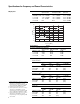
Specifications for Frequency and Power Characteristics Output power Power 250 kHz to 250 MHz > 250 MHz to 1 GHz > 1 to 3 GHz > 3 to 4 GHz > 4 to 6 GHz Option 501-504 +11 to –136 dBm +13 to –136 dBm +10 to –136 dBm +7 to –136 dBm N/A With Option UNB +15 to –136 dBm +17 to –136 dBm +16 to –136 dBm +13 to –136 dBm N/A Option 506 +12 to –136 dBm +14 to –136 dBm +13 to –136 dBm +10 to –136 dBm +10 to –136 dBm Typical maximum available power 26 24 Option UNB Option 506 Power [dB] 22 20 18 16 14 Option 5
Specifications for Frequency and Power Characteristics Level accuracy with digital modulation turned on [relative to CW] Conditions: [with PRBS modulated data; if using I/Q inputs, √ I2 + Q2 = 0.5 Vrms , nominal] 1 Level accuracy with ALC on π/4 DQPSK or QPSK formats Conditions: With raised cosine or root-raised cosine filter and a ≥ 0.35; with 10 kHz ≤ symbol rate ≤ 1 MHz; at RF freq ≥ 25 MHz; power ≤ max specified –3 dB Option 501-504 Option 506 ±0.15 dB ±0.
Specifications for Frequency and Power Characteristics Repeatability and linearity Repeatability 1900 MHz CW, 5 dBm, attenuator hold On, ALC On Repeatability 1900 MHz CW, 5 dBm, attenuator hold Off, ALC Off 0.1 0.5 0.09 0.08 0.4 0.07 0.35 0.06 0.3 Power error (dB) Powererror (dB) 0.45 Typical unit Limits 0.05 0.04 0.25 0.2 0.03 0.15 0.02 0.10 0.01 0.
Specifications for Frequency and Power Characteristics Linearity CW or GSM, 850 MHz, attenuator hold On, ALC On 0.3 Typical STD unit Typical Option UNB unit 0.25 0.2 0.15 Upper limit 0.1 ALC offset error (dB) Linearity measures the accuracy of small changes while the attenuator is held in a steady state (to avoid power glitches). This is useful for fine resolution changes.1 Typical Option 506 unit Lower limit 0.05 0 -0.05 -0.1 -0.15 -0.2 -0.25 Limit is undefined above 13 dBM for STD units.
Specifications for Frequency and Power Characteristics Spectral purity SSB Phase noise [at 20 kHz offset]1 Standard at 500 MHz (< –124 dBc/Hz) at 1 GHz (< –118 dBc/Hz) at 2 GHz (< –112 dBc/Hz) at 3 GHz (< –106 dBc/Hz) at 4 GHz (< –106 dBc/Hz) at 6 GHz N/A With Option UNJ < –135 dBc/Hz, (< –138 dBc/Hz) < –130 dBc/Hz, (< –134 dBc/Hz) < –124 dBc/Hz, (< –128 dBc/Hz) < –121 dBc/Hz, (< –125 dBc/Hz) < –118 dBc/Hz, (< –122 dBc/Hz) < –113 dBc/Hz, (< –117 dBc/Hz) Residual FM1 [CW mode, 0.
Specifications for Frequency and Power Characteristics Characteristic SSB phase noise With Option 1E5 With Option UNJ I/Q on I/Q on CW mode CW mode fc = 850 MHz fc = 850 MHz I/Q on I/Q on CW mode CW mode fc = 1900 MHz fc = 1900 MHz I/Q on I/Q on CW mode CW mode fc = 2200 MHz fc = 2200 MHz I/Q on or CW mode PN mode 1 PN mode 2 Phase noise modes 1 and 2 at fc = 900 MHz fc = 5.
Specifications for Analog Modulation Frequency bands Frequency modulation 1,2 Band 1 2 3 4 5 6 Frequency range N number 250 kHz to ≤ 250 MHz 1 > 250 MHz to ≤ 500 MHz 0.5 > 500 MHz to ≤ 1GHz 1 > 1 to ≤ 2 GHz 2 > 2 to ≤ 4 GHz 4 > 4 to ≤ 6 GHz 8 Maximum deviation3 Standard N x 8 MHz Resolution With Option UNJ N x 1 MHz 0.
Specifications for Analog Modulations Phase modulation 1, 2 Resolution 0.1% of set deviation Modulation frequency response 3, 4 Standard Mode Normal BW High BW6 Maximum deviation N x 80 rad N x 8 rad N x 1.6 rad Allowable rates [3 dB BW] FM path 1 FM path 2 DC to 100 kHz DC to 100 kHz (DC to 1 MHz) (DC to 0.9 MHz) (DC to 10 MHz) (DC to 0.9 MHz) Maximum deviation N x 10 radians N x 1 radians Allowable rates [3 dB BW] FM path 1 FM path 2 DC to 100 kHz DC to 100 kHz (DC to 1 MHz) (DC to 0.
Specifications for Analog Modulation Wideband AM Rates [1 dB bandwidth] 1 ALC on (400 Hz to 40 MHz) ALC off (DC to 40 MHz) Wideband AM using external I input only Pulse modulation Sensitivity 0.5 V = 100% Input impedance 50 Ω, nominal On/off ratio 1 ≤ 4 GHz > 4 GHz > 80 dB (> 64 dB) Rise/fall times1 (150 ns) Minimum width1 ALC on ALC off (2 µs) (0.4 µs) Pulse repetition frequency1 ALC on (10 Hz to 250 kHz) ALC off (DC to 1.0 MHz) Level accuracy 1, 2 [relative to CW at ≤ 4 dBm standard, ≤ 7.
Specifications for Analog Modulation Internal modulation source Provides modulating signal for FM, AM, pulse and phase modulation signals, and provides LF output source for basic function generator capability. Waveforms Sine, square, ramp, triangle, pulse, noise Rate range Sine Square, ramp, triangle 0.1 Hz to 100 kHz 0.1 Hz to 20 kHz Resolution 0.
Specifications for Analog Modulation External burst envelope Input voltage RF On RF Off Linear control range 0V –1.0 V 0 to –1 V On/off ratio1 Condition: Vin below –1.05 V ≤ 4 GHz > 4 GHz > 75 dB (> 64 dB) Rise/fall time1 Condition: With rectangular input (< 2 µs) Minimum burst repetition frequency1 ALC on (10 Hz) ALC off DC Composite modulation Simultaneous modulation 1. Parentheses denote typical performance.
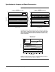
Specifications for I/Q Characteristics I/Q modulation bandwidth I/Q inputs Input impedance Full scale input 1 50 Ω or 600 Ω √ I2 + Q2 = 0.5 Vrms I/Q bandwidth using external I/Q source (ALC off) 2 3.00 850 MHz carrier 1.00 -1.00 [dB] -3.00 1900 MHz carrier -5.00 -7.00 2200 MHz carrier 1800 MHz carrier -9.00 -11.00 -13.00 -15.00 -150 -100 -50 0 50 100 150 Frequency offset from carrier [MHz] I/Q bandwidth using internal I/Q source (Options 001, 002, 601, 602) 3.00 1.00 -1.00 [dB] -3.00 -5.
Specifications for I/Q Characteristics I/Q adjustments Source I/Q baseband inputs Parameter Impedance I offset [600 Ω only] Q offset [600 Ω only] Range 50 or 600 Ω ±5V ±5V I/Q baseband outputs I/Q offset adjustment I/Q offset resolution I/Q gain balance I/Q attenuation I/Q low pass filter ±3V 1 mV ± 4 dB 0 to 40 dB 40 MHz, through RF output I/Q offset adjustment I/Q gain balance I/Q attenuation I/Q quad skew [≤ 3.3 GHz] [> 3.
Specifications for I/Q Characteristics Clock Sample rate Resolution Accuracy 1 Hz to 100 MHz 0.001 Hz Same as timebase +2-42 [in non-integer applications] Baseband filters 40 MHz 2.
Specifications for I/Q Characteristics Baseband generator [real-time mode] [Option 601 or 602] Basic modulation types [custom format] PSK BPSK, QPSK, OQPSK, π/4DQPSK, 8PSK, 16PSK, D8PSK MSK User-defined phase offset from 0 to 100° ASK User-defined depth from 0.001 to 100% QAM 4, 16, 32, 64, 128, 256 FSK Selectable: 2, 4, 8, 16 level symmetric, C4FM User defined: Custom map of up to 16 deviation levels Symbol rate < 5 MHz > 5 MHz, < 50 MHz Maximum deviation 4 times symbol rate 20 MHz Resolution: 0.
Specifications for I/Q Characteristics Data types Internally generated data Pseudo-random patterns Repeating sequence Direct-pattern RAM [PRAM] Max size Option 601 Option 602 PN9, PN11, PN15, PN20, PN23 Any 4-bit sequence Other fixed patterns 8 Mbits 64 Mbits [each bit uses an entire sample space] Use Non-standard framing User file Max size Option 601 800 kB Option 602 6.
Specifications for Signal Personality Characteristics IS-95 CDMA [arbitrary waveform mode 1] [Option 401] Spurious emissions [dBc, IS-95 modified filter with equalizer and amplitude = ≤ -5 dBm standard, ≤ -3 dBm for Option 506, ≤ 0 dBm for Option UNB] 2 0.885 to 1.25 MHz Option 506 1.25 to 1.98 MHz 1.
Specifications for Signal Personality Characteristics Enhanced multitone1 [arbitrary waveform mode] [Option 408] Number of tones 2 to 1024 Tone spacing 1 kHz to 50 MHz, limited by 80 MHz I/Q bandwidth Tone power (relative) 0 to –50 dB Phase distribution Fixed, random or parabolic Suppression level –50 to –90 dBc, depending on number of tones and available calibration time.
Specifications for Signal Personality Characteristics 802.11 WLAN [arbitrary waveform mode] [Option 417]1 EVM (< 1%, –40 dB) The EVM was measured with an 89641A vector signal analyzer with Option B7R. Instrument and software settings listed below.
Specifications for Signal Personality Characteristics Custom modulation Custom digitally modulated signals [real-time mode] 1, 2 [real-time mode] Modulation Filter Filter factor [a or BbT] Modulation index Symbol rate [Msym/s] fc = 1 GHz fc = 2 GHz fc = 3 GHz fc = 4 GHz fc = 5 GHz fc = 6 GHz π/4DQPSK 16QAM Root Nyquist 0.25 0.25 0.25 N/A N/A N/A 4 4 4 Error vector magnitude3, 4 [% rms] 1.1 (0.7) 1.1 (0.7) 1.0 (0.6) 1.2 (0.8) 1.2 (0.8) 1.0 (0.6) 1.6 (1.0) 1.6 (1.0) 1.5 (0.9) 2.5 (1.4) 2.5 (1.3) 3.3 (1.
Specifications for Signal Personality Characteristics GSM/GPRS [real-time mode] [Option 402] Multiframe output data generation Coding scheme Full-rate speech [TCH/FS] CS-1, CS-4 Data PN9 or PN15 The selected data sequence is coded continuously across the RLC data block as per ETSI TS 100 909, 3GPP TS 05.03, V8.9.0, 2000-11 [release 1999] An independent version of the selected data sequence is coded across the MAC header. Frame structure 26-frame multi-frame structure as per ETSI GSM, 05.01 version 6.1.
Specifications for Signal Personality Characteristics EDGE/EGPRS [real-time mode] [Option 402] Multiframe output data generation Coding scheme MCS-1: uplink and downlink, MCS-5: uplink and downlink, MCS-9: uplink and downlink, E-TCH/F43.2 Data PN9 or PN15 The selected data sequence is fully coded continuously across the RLC data blocks according to MCS-1, MCS-5, MCS-9 or E-TCH/F43.2.
Specifications for Signal Personality Characteristics GSM/EDGE base station bit error rate test [BERT] [Option 300] This is a system of two instruments; an ESG with Option 300, and a VSA with Option 300. Both are required. Option 300 for the ESG requires Option 601 or 602, the TDMA personalities [Option 402], and the UN7 BER board. The VSA functions as an IF downconverter. It may be used simultaneously to make transmitter measurements on the loop back signal.
Specifications for Signal Personality Characteristics Bit error rate [BER] analyzer [Option UN7] Clock rate 100 Hz to 60 MHz Supported data patterns PN9, 11, 15, 20, 23 Resolution 10 digits Bit sequence length 100 bits to 4.294 Gbits after synchronization Features Input clock phase adjustment and gate delay Adjustable input threshold Hi/lo threshold selectable from 0.7 V [TTL], 1.4 V [TTL] 1.65 V [CMOS 3.3], 2.5 V [CMOS 5.
General Characteristics Operating characteristics Power requirements 90 to 254 V; 50, or 60 Hz; 300 W maximum, power factor corrected. Not for 400 Hz use.1 Operating temperature range2 0 to 55 °C Storage temperature range –40 to 71 °C Shock and vibration Meets MIL-STD-28800E Type III, Class 3. Leakage Conducted and radiated interference meets MIL-STD-461C CE02 Part 2 and CISPR 11. Leakage is typically < 1 µV [nominally 0.
General Characteristics Accessories Transit case Part number 9211-1296 Inputs and outputs All front panel connectors can be moved to rear with Option 1EM. 10 MHz input Accepts a 1, 2, 5, or 10 MHz ±10 ppm [standard timebase] or ±1 ppm [high-stability timebase] reference signal for operation with an external timebase. Nominal input level –3.5 to +20 dBm, impedance 50 ohms. [BNC, rear panel] 10 MHz output Outputs the 10 MHz reference signal. Level nominally +3.9 dBm ±2 dB.
General Characteristics Data clock input The CMOS1 compatible data clock connector accepts an externally supplied data-clock input for digital modulation applications. The expected input is a bit clock signal where the falling edge is used to clock the data and symbol sync signals. The maximum clock rate is 50 MHz. The damage levels are –0.5 to +5.5 V. This female BNC connector is provided on signal generators with Option 601 or 602.
General Characteristics External 1 input This BNC input connector accepts a ±1 Vpeak signal for AM, FM, pulse, burst, and phase modulation. For all these modulations, ±1 Vpeak produces the indicated deviation or depth. When ac-coupled inputs are selected for AM, FM, or phase modulation and the peak input voltage differs from 1 Vpeak by more than 3%, the hi/lo annunciator light on the display. The input impedance is 50 ohms and the damage levels are 5 Vrms and 10 Vpeak .
General Characteristics _ _ I and Q out _ _ I and Q are used in conjunction with I and Q to provide a balanced baseband stimulus. Balanced signals are signals present in two separate conductors that are symmetrical about the common mode offset, and are opposite in polarity [180 degrees out of phase]. These female BNC connectors are provided only on signal generators with Option 601 or 602. If you configure your signal generator with Option 1EM, these inputs are relocated to rear panel SMB connectors.
General Characteristics With Option UN7 BER data, BER clock BER gate Accepts CMOS 1 or 75 Ω input. Polarity is selected. Clock duty and inputs cycle is 30% to 70%. [SMB, rear panel] BER sync loss output Outputs a CMOS1 signal that is low when sync is lost. Valid only when measure end signal is high. [Auxiliary I/O connector, rear panel] BER no data output Outputs a CMOS1 signal that is low when no data is detected. Valid only when measure end is high.
General Characteristics RS-232 connector This male DB-9 connector is an RS-232 serial port that can be used for controlling the signal generator remotely. It is functionally equivalent to the GPIB connector. The following table shows the description of the pinouts. The pin configuration is shown below.
Ordering Information1 Frequency options Performance enhancement options • • • • • 501 502 503 504 506 • UNB • UNJ • 1E5 • 1EM • 0032 • 0042 • 601 • 602 • 0053 • UN7 • 300 Signal creation software 3, 6 Baseband Studio products 4 System accessories 1 GHz frequency range 2 GHz frequency range 3 GHz frequency range 4 GHz frequency range 6 GHz frequency range [requires option UNJ, includes mechanical attenuator] High output power with mechanical attenuator [included with 506] Enhanced phase noise perform
Related Literature Application literature • RF Source Basics, a self-paced tutorial (CD-ROM), literature number 5980-2060E. • Digital Modulation in Communications Systems—An Introduction, Application Note 1298, literature number 5965-7160E. • Using Vector Modulation Analysis in the Integration, Troubleshooting and Design of Digital Communications Systems, Product Note, literature number 5091-8687E. • Testing CDMA Base Station Amplifiers, Application Note 1307, literature number 5967-5486E.
See the ESG Web page for the latest information Get the latest news, product and support information, application literature, firmware upgrades and more. Agilent’s Internet address for the ESG is: www.agilent.com/find/esg Agilent Email Updates www.agilent.com/find/emailupdates Get the latest information on the products and applications you select. Agilent Direct www.agilent.com/find/agilentdirect Quickly choose and use your test equipment solutions with confidence. Agilent Open www.agilent.