
User manual


AS bus 2 is intended to connect modules of the same type, i.e. of the same model number, although some exceptions
to this rule might be possible. If modules with the same model number, but different memory length options, are
connected only the shortest memory length can be used.
The AS bus 2 connector is located on the front panel of each module. Bridges are used to connect adjacent modules
for synchronization. An AS bus 2
multi-instrument is activated through software by a function call. Up to 5 6U
modules, or 3 3U modules, may be synchronized with the AS bus 2. More detailed information and the commands
required to set up the AS bus 2 clock and trigger distribution are included in the Programmer's Guide and Reference
manuals.
3.8. Special Front Panel Inputs and Controls
Connector Function
MMCX CLK IN 50 Ω External Reference or External Clock Input
MMCX I/O A User configurable (see below)
MMCX TR OUT Signal occurs after an accepted TRIGGER.
MMCX I/O B User configurable (see below)
The I/O A and I/O B signals are 3.3 V compatible CMOS. This means that, on input, low is < 0.7 V and high must be
in the range [1.7 V, 5.0 V]. An unconnected signal will be high. This definition ensures TTL compatibility. On
output, the low level will be in the range [0 V, 0.7 V] and the high level in the range [1.7 V, 3.3 V] for HiZ. The high
level output will typically give 0.8 V into 50 Ω. The I/O A or B connectors can be used for an Enable trigger input or
the following output signals: 10 MHz reference clock, Acquisition skipping to next segment, Acquisition is active,
Trigger is armed.
3.9. External Trigger Output
When the digitizer is ready to be triggered and a valid trigger signal occurs, a trigger output is generated for external
use. It is always available on the Front Panel Trigger Out MMCX connector. The pulse ends when the data
acquisition for the trigger in question is complete.
NOTE: The External Trigger Output functionality is implemented in the hardware. No Trigger Out signal occurs for
software-generated triggers such as those of the AUTO mode of AcqirisLive or through the use of the function
AcqrsD1_forceTrigger. However, AcqrsD1_forceTriggerEx does generate the signal.
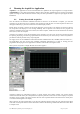
Trigger Output Block diagram:
The output swing is 1.6 V (± 0.8 V) when
unloaded and 0.8 V when terminated on 50
Ω. The rise and fall times are 2.5 ns typical.
The offset can be adjusted, by software
control in the range [–2.3 V, +2.3 V]
unloaded, or [-1.15 V, +1.15 V] into 50 Ω.
The maximum output current capability is ±
15 mA. As the output is retro-terminated, it
is possible to drive a 50 Ω line unterminated
(HiZ) without loss of performance.
Signal: 1.6V swing
0v centered
Offset: +/-2.5 V
G=1
50 Ohm
Trigger Out
For a TTL compatible signal, set the offset
to 1.0 V and the swing at destination will be
+0.2 to +1.8 V.
For an ECL compatible signal, terminated
on 50 Ω to –1.2 V, set the offset to –1.2 V
and the output will be in the range [–0.8 V, –
1.6 V
]).
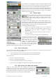
Alternatively, to reduce the current drawn from the digitizer, the terminations shown here can be used:
A standardized trigger out signal can also be routed to the PXI Bus Star Trigger line.
R
68
R
220
-5V
GND
Trigger
Out
With
Offset
-1.18V
R
68
R
220
+5V
ECL
Signal
TTL
signal
GND
Trigger O ut
With
Offset
+1.18V
User Manual: Agilent Acqiris 10-bit Digitizers Page 24 of 43