
User`s manual


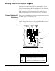

Writing to the
Control Register
To write to the Control Register from the backplane data lines, you must
implement the following signal and control lines:
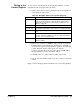
1. Address the module correctly by placing the data shown in Table 3-4
on the backplane address lines:
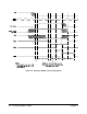
Table 3-4. Backplane Address Lines (Control Register)
Lines Data Required
Lines A1-A3 Must be set low/high/low (010) to select the BASE+4 enable line.
BASE + 4 set low provides an enable function at U2B for Control
Register drivers U15/U16 to be clocked by the LATCH pulse (see
Table 2-2 on page 34).
Lines A4, A5 Must both be low (0) to enable the 3-to-8 line decoder U21.
Lines A6 - A13 Must equal the logical address of the module as set on DIP switch SW1.
Lines A14, A15 Must always be set high (1) to access the upper 16K of address
space.
Lines AM0 - AM5 Must be set to either hexadecimal 29 (10 1001) or hexadecimal 2D
(10 1101). Refer to the
VMEbus Specification (Table 2-3) and the
VXIbus Specification (Rule C.2.10).
Line LWORD* Must always be set false (1) since this is a D16 device (short word
transfer = 16-bits).
2. This is a write operation, so WRITE* must go true (0) to provide the
LATCH signal from the DTACK state machine in U9. LATCH is a
one clock-cycle negative-going pulse that is applied to the other input
to U2B. With both inputs to U4A set low, the output is a
positive-going pulse that clocks the control data from DB0 - DB15
through U22/U23 to access points CTL2 - CTL15.
3. Set IACK* false (1) to enable address equality detector U18.
4. Set both data strobes DS0* and DS1* true (0) to indicate a 16-bit data
transfer.
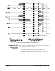
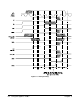
Figure 3-4 shows timing required for the PAL (U9) control and signal lines.
Chapter 3 Using the Agilent E1490C 55