
User`s manual
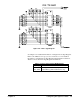
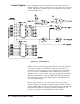
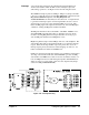
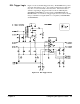


Table 2-8. Control Register Bit Definitions
Data Bit(s) Definitions
CR0 (1 = Reset the module, User defines reset actions)
CR1 (1 = inhibit setting of SYSFAIL*; if Reset = 1, safe)
CR2 - CR14 Device Dependent (User Assignable)
CR15 (1 = Enable access to A24/A32 Registers; 0 = Disable)
See pages 54 and 55 for additional information on using the Control Register.
Refer to the VXIbus System Specification, Section C.2.1.1.2 for detailed
information concerning Control Register implementation restrictions.
DTACK, Interrupt,
and Control
A programmable array logic IC (PAL) provides the timing and control
signals for standard data transfer cycles and interrupt
requests/acknowledgements. Hardware and software reset signals, together
with a card fail signal, have also been implemented.
DTACK The Data Transfer ACKnowledge (DTACK) circuitry is centered around the
PAL (U9). A state machine in the PAL controls all read and write data
transfer cycles. Operation begins with the state machine in the idle state.
See Figure 2-25 for the following discussion.
In the first part of the transfer cycle, the system controller places the address of
the breadboard module on the backplane address lines A1 - A15 and address
modifier lines AM0 - AM5, and then sets the appropriate data strobe lines true
(DS0* and DS1* for a D16 device). When the address equality detectors (U17,
U18) detect the address match, the output of U17 goes low.
This low is felt at the Card ADDRess (CADDR) input to U9 which, together
with the active data strobes, tells the DTACK state machine in the PAL that the
module has been addressed for a data transfer cycle. This starts the state
machine, with all signals being clocked by SYSCLK (16 MHz).
In the first active state, the data bus drivers (U19 and U20) are enabled and the
register-specifier part of the address (A1 - A5) is latched onto the outputs of U8
using the Data Bus ENable (DBEN) output of U9. If the data transfer cycle is a
read operation (as indicated by WRITE* false), the decoded output of U7
(enabled by the output of equality detector U17) determines which one of the
registers (Status, ID, or Device Type) is enabled to put its contents onto the
module’s internal data bus (DB0 - DB15).
The next state then generates a high at the DTACK output of U9. This
forces DTACK* true on the backplane through U5B, acknowledging to the
system controller that the module has received the request for data and has
placed the contents of the specified register onto the data lines. With U19
and U20 enabled, internal data lines DB0 - DB15 are connected directly to
the backplane data lines D0 - D15.
Chapter 2 Configuring the Agilent E1490C 41