
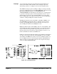
User`s manual
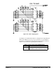
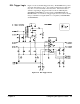

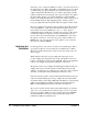

Control Register The Control Register is a 16-bit register which, when written to from the
backplane data bus, causes specific actions to be executed by the breadboard
module. The primary components of the Control Register are U22 and U23
as shown in Figure 2-24.
Table 2-8 shows the Control Register bit definitions. The Control Register
is selected for writing to by the BASE + 4 enable line (see Table 2-2).
STATUS* going low at the input of U4A, combined with a negative pulse
(for one clock cycle of SYSCLK) from the LATCH* output of U9 (also
applied to U4A), provides a positive-going edge clocking pulse to U22/U23.
This pulse clocks whatever is present on DB0 - DB15 through U22/U23 to
the Control Register access points (CTL2 - CTL15). CTL0 and CTL1 are
reset and sysfail inhibit bits.
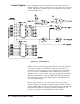
The user may connect any or all of these points to his custom circuitry,
keeping in mind the pre-defined bit assignments shown in Table 2-8. Data
present on DB0 - DB15 would have been written there by the same DTACK
state machine data transfer cycle that provided the LATCH pulse. See
page 41 for a discussion of the DTACK state machine operation.
Figure 2-24. Control Register
40 Configuring the Agilent E1490C Chapter 2