
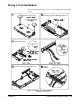
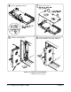
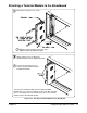
User`s manual
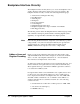
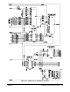
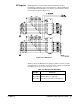

Data Bus Drivers The Agilent E1490C breadboard module is designed to be used as an A16 and
a D16 device only. As such, only backplane address lines A1 - A15 and data
lines D0 - D15 have been implemented on the module. VXIbus backplane
connector J1 contains 16 bi-directional data lines labeled D0 through D15. The
module connects to these data lines using the circuitry shown in Figure 2-20.
Data buffering is provided for the data lines by two tri-state octal bus
transceivers. U20 buffers D0 through D7 and U19 buffers D8 through D15.
Note that the data lines are labeled DB0 through DB15 on the module side
of the buffers. U19 and U20 are enabled during a data bus transfer cycle
when DBEN (Data Bus ENable) goes low. This occurs whenever the
breadboard module is correctly addressed by a match of the module’s
logical address as set by SP1 (0-7).
The direction of data transfer is determined by WRITE*. When WRITE* is
true (a "write" operation), information present on backplane lines D0 - D15
is transferred to the breadboard module via DB0 - DB15. When WRITE* is
false (a "read" operation), information present on DB0 - DB15 is transferred
to backplane lines D0 - D15.
During a normal read operation, the information present on DB0 - DB15 is
selected by the Address Decode circuitry from one of three sources:
– Status Register (U24/U25)
– ID Register (U11/U12)
– Device Type Register (U14/U13)
User-supplied circuitry can decode the entire module address space,
allowing for 32 registers, maximum. Refer to Table 2-2 and Figure 2-19.
Figure 2-20. Data Bus Drivers
Chapter 2 Configuring the Agilent E1490C 35