
User`s manual

Either of the two address modifier hexadecimal codes indicated above will
establish A16 addressing per the VXIbus System Specification (Section
C.2.1.1.5). In the VXIbus addressing scheme for an A16 device, A14 and
A15 are always set to 1 to select the upper 16K of the 64K A16 address
space (per the VXIbus System Specification, Sections A.2.3.3 and C.2.1.1.1).
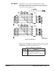
LWORD* is false when decoding short word (16-bit) transfers.
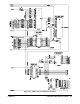
If a second match occurs at U17, its output goes low. This triggers a data
transfer cycle using the DTACK state machine in the DTACK Interrupt
Control IC (PAL) by the low at U9 input CADDR. See page 41 for more
information on the DTACK state machine. As part of the data transfer
cycle, U9 sets DBEN low, latching the remaining backplane address lines
(A1 - A5) at the U8 outputs to the two 3-to-8-line decoders (U7 and U6).
Latch U8 ensures that the address information is held valid until the data
strobes go false even though the address lines may no longer be valid.
U7 is enabled if G1 is high and both G2A and G2B are low. Therefore, A4
and A5 must both be low to select a register for connection to the data bus
(D0 - D15). G1 will be high if there was a match at U18 (via U15D). If U7
is enabled, backplane lines A1 - A3 are decoded to specify which register
(Status, ID, Device Type, or Control) is to be connected to the data bus.
User-supplied circuitry can decode the entire module address space.
This can provide up to 32 registers maximum. If additional decoding is
necessary, A4 and A5 are accessible on the module. See Table 2-2.
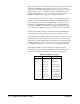
Table 2-2. Register Selection
A3 A2 A1 Enable Line Register
0 0 0 Base + 0 ID
0 0 1 Base + 2 Device Type
0 1 0 Base + 4 Status/Control
0 1 1 Base + 6 User Assignable
1 0 0 Base + 8 User Assignable
1 0 1 Base + A User Assignable
1 1 0 Base + B User Assignable
1 1 1 Base + C User Assignable
34 Configuring the Agilent E1490C Chapter 2