Agilent 4291B RF Impedance/Material Analyzer SERVICE MANUAL SERIAL NUMBERS This manual applies directly to instruments with serial number pre x JP1KE, or rmware revision 01.00. For additional important information about serial numbers, read \ANALYZERS COVERED BY THIS MANUAL" in General Information of this service manual. Agilent Part No.
Notice The information contained in this document is subject to change without notice. This document contains proprietary information that is protected by copyright. All rights are reserved. No part of this document may be photocopied, reproduced, or translated to another language without the prior written consent of the Agilent Technologies Company. Agilent Technologies Japan, Ltd.
Manual Printing History The manual printing date and part number indicate its current edition. The printing date changes when a new edition is printed. (Minor corrections and updates that are incorporated at reprint do not cause the date to change.) The manual part number changes when extensive technical changes are incorporated.
Safety Summary The following general safety precautions must be observed during all phases of operation, service, and repair of this instrument. Failure to comply with these precautions or with speci c WARNINGS given elsewhere in this manual violates safety standards of design, manufacture, and intended use of the instrument. The Agilent Technologies Company assumes no liability for the customer's failure to comply with these requirements.
DO NOT Substitute Parts Or Modify Instrument Because of the danger of introducing additional hazards, do not substitute parts or perform unauthorized modi cations to the instrument. Return the instrument to a Agilent Technologies Sales and Service O ce for service and repair to ensure the safety features are maintained. Dangerous Procedure Warnings Warnings , such as the example below, precede potentially dangerous procedures throughout this manual. Instructions contained in the warnings must be followed.
Typeface Conventions Bold Boldface type is used when a term is de ned. For example: icons are symbols. Italic type is used for emphasis and for titles of manuals and other publications. Italic type is also used for keyboard entries when a name or a variable must be typed in place of the words in italics. For example: copy lename means to type the word copy, to type a space, and then to type the name of a le such as file1. Computer font is used for on-screen prompts and messages.
Certi cation Agilent Technologies Company certi es that this product met its published speci cations at the time of shipment from the factory. Agilent Technologies further certi es that its calibration measurements are traceable to the United States National Institute of Standards and Technology, to the extent allowed by the Institution's calibration facility, or to the calibration facilities of other International Standards Organization members.
Exclusive Remedies The remedies provided herein are buyer's sole and exclusive remedies. Agilent Technologies shall not be liable for any direct, indirect, special, incidental, or consequential damages, whether based on contract, tort, or any other legal theory. Assistance Product maintenance agreements and other customer assistance agreements are available for Agilent Technologies products. For any assistance, contact your nearest Agilent Technologies Sales and Service O ce.
Contents 1. General Information INTRODUCTION . . . . . . . . . . . . ORGANIZATION OF SERVICE MANUAL . ANALYZERS COVERED BY MANUAL . . TABLE OF SERVICE TEST EQUIPMENT . . . . . . . . . . . . . . . . . . . . . . . . . . . . . . . . . . . . . . . . . . . . . . . . . . . . . . . . . . . . . . . . . . . . . . . . . . . . . 1-1 1-1 1-3 1-4 INTRODUCTION . . . . . . . . . . . . . . . . GENERAL INFORMATION . . . . . . . . . . . Warm Up Time . . . . . . . . . . . . . . . Ambient Conditions . . .
Norm-Temp High-Impedance Test Head . . . . . . Norm-Temp Low-Impedance Test Head (Option 012) High-Temp High-Impedance Test Head (Option 013) High-Temp Low-Impedance Test Head (Option 014) . Measurement Accuracy Test . . . . . . . . . . . . Norm-Temp High-Impedance Test Head . . . . . . Norm-Temp Low-Impedance Test Head (Option 012) High-Temp High-Impedance Test Head (Option 013) High-Temp Low-Impedance Test Head (Option 014) . DC Bias Accuracy Test . . . . . . . . . . . . . . . . . . . . . . . . . . . .
Procedure . . . . . . . . . . . . . . . . . . . . . . . . . . . . . . . . DC BIAS LEVEL CORRECTION CONSTANTS (OPTION 001 ONLY) . . . . . . . Procedure . . . . . . . . . . . . . . . . . . . . . . . . . . . . . . . . 10 MHz REFERENCE OSCILLATOR FREQUENCY ADJUSTMENT (OPTION 1D5 ONLY) . . . . . . . . . . . . . . . . . . . . . . . . . . . . . . . . . Required Equipment . . . . . . . . . . . . . . . . . . . . . . . . . . . Procedure . . . . . . . . . . . . . . . . . . . . . . . . . . . . . . . . 4.
4. Remove Assemblies . . . . . . . . . . . . . . . . . . . TROUBLESHOOT THE FAN AND THE A50 DC-DC CONVERTER 1. Troubleshoot the Fan . . . . . . . . . . . . . . . . . . 2. Troubleshoot the A50 DC-DC Converter . . . . . . . . . TROUBLESHOOT THE A2 POST-REGULATOR . . . . . . . . . 1. Check the A40 Pre-Regulator . . . . . . . . . . . . . . 2. Check the A50 DC-DC Converter . . . . . . . . . . . . . 3. Remove Assemblies . . . . . . . . . . . . . . . . . . . 4. Measure the A2 Post Regulator Output Voltages . . . .
1. Check the A3A3 RF Signal . . . . . . . . . . . . . . . CHECK A7 OUTPUT ATTENUATOR CONTROL SIGNALS . . . 1. Check A7 Control Signals . . . . . . . . . . . . . . . CHECK A22 DC BIAS 1/2 OUTPUT . . . . . . . . . . . . . 1. Check A22 Output Voltages . . . . . . . . . . . . . . CHECK THE A60 HIGH STABILITY FREQUENCY REFERENCE . . . . . . . . . . . . . . . . . . . . . . . . . . . . . . . . . . . . . . . . . . . . . . . . . . . . . . 7-27 7-29 7-29 7-31 7-31 7-33 . . . . . . . . . . . . . . . . . .
11: A3A1 DIVIDER . . . . . . . . . . . . . . . . . . 12: A6 3RD LO OSC . . . . . . . . . . . . . . . . . . 13: A3A1 SOURCE OSC . . . . . . . . . . . . . . . . 14: A6 SEQUENCER . . . . . . . . . . . . . . . . . . 15: SOURCE LEVEL . . . . . . . . . . . . . . . . . . 16: DC BIAS . . . . . . . . . . . . . . . . . . . . . EXTERNAL TESTS . . . . . . . . . . . . . . . . . . . 17: FRONT PANEL DIAG. . . . . . . . . . . . . . . . 18: DSK DR FAULT ISOL'N . . . . . . . . . . . . . . . 19: POWER SWEEP LINEARITY . . . .
NNNNNNNNNNNNNNNNNNNNNNNNNNNNNNNN WAIT COUNT (:DIAG:SERV:BUS:WAIT ) . . . . . . . . . . Bus Measurement . . . . . . . . . . . . . . . . . . . . . . . . . . Bus Measurement Procedure . . . . . . . . . . . . . . . . . . . . . Bus Measurement Values . . . . . . . . . . . . . . . . . . . . . . . DC Bus Node Descriptions . . . . . . . . . . . . . . . . . . . . . . 0: OFF . . . . . . . . . . . . . . . . . . . . . . . . . . . . . . 1: +5 V (AUX) (2.025 U) . . . . . . . . . . . . . . . . . . . . . .
OSC CONTROL MENU . . . . . . . . . . . . . . . . . . . . . . . OSC AUTO man (:DIAG:SERV:SOUR:MODE {AUTO|MAN}) . . . . . . . OUTPUT ATT [ ] (:DIAG:SERV:SOUR:ATT {AUTO|DB0|DB10|DB20|DB30|DB40|DB50|DB60} ) . . . . . . . . OSC DAC AUTO man (:DIAG:SERV:SOUR:LEV:DAC:MODE {AUTO|MAN}) OSC DAC VALUE (:DIAG:SERV:SOUR:LEV:DAC:VAL ) . . OSC OUT ON off (:DIAG:SERV:SOUR:STAT {OFF|ON|0|1} ) . . . . DC BIAS CONTROL MENU . . . . . . . . . . . . . . . . . . . . . DC BIAS AUTO man (:DIAG:SERV:DCB:MODE {AUTO|MAN}) . .
A30 Front-Panel Keyboard . . . . . . . . . . . . . . . A31 I/O Connector . . . . . . . . . . . . . . . . . . . A32 I-BASIC Interface . . . . . . . . . . . . . . . . . A51 GSP . . . . . . . . . . . . . . . . . . . . . . . A52 LCD (Liquid Crystal Display) . . . . . . . . . . . . A53 FDD . . . . . . . . . . . . . . . . . . . . . . . A54 Inverter . . . . . . . . . . . . . . . . . . . . . SOURCE THEORY . . . . . . . . . . . . . . . . . . . . A5 Synthesizer . . . . . . . . . . . . . . . . . . . . REF OSC . . . .
13. Replacement Procedures INTRODUCTION . . . . . . . . . . . . . . . . . . . . . . . . . . . . . . TOP COVER REMOVAL . . . . . . . . . . . . . . . . . . . . . . . . . . . Tools Required . . . . . . . . . . . . . . . . . . . . . . . . . . . . . . Procedure . . . . . . . . . . . . . . . . . . . . . . . . . . . . . . . . BOTTOM COVER REMOVAL . . . . . . . . . . . . . . . . . . . . . . . . Tools Required . . . . . . . . . . . . . . . . . . . . . . . . . . . . . . Procedure . . . . . . . . . . . . . . . . . .
Tools Required . . . . . . . . . . . . . . . . Removal Procedure . . . . . . . . . . . . . Replacement Procedure . . . . . . . . . . . A52 LCD REPLACEMENT . . . . . . . . . . . Removal Procedure . . . . . . . . . . . . . A53 FDD REPLACEMENT . . . . . . . . . . . Tools Required . . . . . . . . . . . . . . . . Removal Procedure . . . . . . . . . . . . . A60 FREQ REF REPLACEMENT . . . . . . . . Tools Required . . . . . . . . . . . . . . . . Removal Procedure . . . . . . . . . . . . . TEST HEAD REPLACEMENT . .
Figures 1-1. 2-1. 2-2. 2-3. 2-4. 2-5. 2-6. 2-7. 3-1. 3-2. 3-3. 3-4. 3-5. 3-6. 3-7. 3-8. 3-9. 3-10. 3-11. 3-12. 3-13. 3-14. 3-15. 3-16. 3-17. 3-18. 3-19. 3-20. 3-21. 4-1. 4-2. 4-3. 4-4. 5-1. 5-2. 5-3. 5-4. 5-5. 5-6. 5-7. 5-8. 5-9. 5-10. 5-11. 5-12. 5-13. Serial Number Plate . . . . . . . . . . . . . . . . . . . Frequency Accuracy Test Setup . . . . . . . . . . . . . . OSC Level Accuracy Test Setup . . . . . . . . . . . . . . Measurement Accuracy Test Setup . . . . . . . . . . . .
5-14. 6-1. 6-2. 6-3. 7-1. 7-2. 7-3. 7-4. 7-5. 7-6. 7-7. 7-8. 7-9. 7-10. 7-11. 7-12. 7-13. 7-14. 7-15. 7-16. 7-17. 7-18. 7-19. 7-20. 7-21. 7-22. 7-23. 7-24. 7-25. 8-1. 8-2. 8-3. 9-1. 9-2. 9-3. 9-4. 9-5. 10-1. 10-2. 10-3. 10-4. 10-5. 10-6. 10-7. 10-8. 10-9. 10-10. 10-11. 10-12. 10-13. 10-14. 10-15. 10-16. 10-17. 11-1. Power Supply Block Diagram 3 . . . . . . . . . . . . . . Digital Control Group Simpli ed Block Diagram . . . . . . A1 Eight LEDs' Pattern . . . . . . . . . . . . . . . . . Bootloader Display .
11-2. 11-3. 11-4. 11-5. 11-6. 11-7. 11-8. 11-9. 11-10. 11-11. 12-1. 12-2. 12-3. 12-4. 12-5. 12-6. 12-7. 12-8. 12-9. 12-10. 12-11. 12-12. 12-13. 12-14. 12-15. 12-16. 12-17. 12-18. 13-1. 13-2. 13-3. 13-4. 13-5. 13-6. 13-7. 13-8. 13-9. 14-1. 14-2. A-1. B-1. Power Supply Functional Group, Simpli ed Block Diagram A2 Eight Status LED . . . . . . . . . . . . . . . . . . Digital Control Group, Simpli ed Block Diagram . . . . . Source Simpli ed Block Diagram . . . . . . . . . . . .
Tables 1-1. 2-1. 2-2. 2-3. 2-4. 3-1. 4-1. 4-2. 4-3. 5-1. 5-2. 7-1. 7-2. 7-3. 7-4. 7-5. 9-1. 10-1. 10-2. 11-1. 11-2. 11-3. 12-1. 12-2. 12-3. 12-4. 12-5. 12-6. 12-7. 12-8. 12-9. 12-10. 12-11. 12-12. 12-13. 12-14. 12-15. 12-16. 12-17. 12-18. 12-19. 12-20. 12-21. 12-22. 12-23. 12-24. Recommended Test Equipment . . . . . . . . . . . . Test Setting for Normal Temperature Test Heads . . . . Test Setting for High Temperature Test Heads . . . . . DC Bias Voltage Accuracy Test Settings . . . . . . . .
12-25. 12-26. 12-27. 14-1. A-1. A-2. B-1. High Temp. Test Heads Parts (Fixture Side, Option 014) . . . . . High Temp. Test Heads Parts (Test Station Side, Opt. 013 and 014) High Temp. Test Heads Parts (Fixture Stand) . . . . . . . . . . . Post Repair Procedures . . . . . . . . . . . . . . . . . . . . . Manual Changes by Serial Number . . . . . . . . . . . . . . . Manual Changes by Firmware Version . . . . . . . . . . . . . . Fuse Selection . . . . . . . . . . . . . . . . . . . . . . . . . Contents-16 . .
1 General Information INTRODUCTION The Service Manual is a guide to servicing the 4291B RF Impedance/Material Analyzer. The manual contains information required to performance test, adjust, troubleshoot, and repair the analyzer. ORGANIZATION OF SERVICE MANUAL This manual consists of the chapters and appendices listed below. They are divided by tabs. This section lists the names of the tabs and the describes content of each chapter and the appendices. Performance Tests.
Theory of Operation. Explains the overall operation of the analyzer, the division into functional groups, and the operation of each functional group. Replaceable Parts. Provides part numbers and illustrations of the replaceable assemblies and miscellaneous chassis parts, together with the ordering information. Replacement Procedures. Provides procedures to disassemble portions of the analyzer when certain assemblies have to be replaced. Post-Repair Procedures.
ANALYZERS COVERED BY MANUAL Agilent Technologies uses a two-part, ten-character serial number that is stamped on the serial number plate (see Figure 1-1) attached to the rear panel. The rst ve digits are the serial pre x and the last ve digits are the su x. The same pre x is used for all identical instruments. The pre x changes only when a change is made to the instrument. However, the su x is assigned sequentially and is unique to each instrument.
TABLE OF SERVICE TEST EQUIPMENT The rst part of Table 1-1 lists all of the equipment required to performance test, adjust, and troubleshoot the analyzer. The table also notes the use and critical speci cations of each item, and the recommended models. Equipment other than the recommended models may be substituted if the equipment meets or exceeds the critical speci cations.
Table 1-1.
2 Performance Tests INTRODUCTION This chapter provides the 4291B RF Impedance/Material Analyzer performance tests. These performance tests are used to verify that the analyzer's performance meets its speci cations. General information about the performance tests is provided rst. Then, step by step procedures for each test are provided. The each test procedure consists of the following parts: Description: Describes the test procedure. Speci cation: Describes the performance veri ed in the test.
Recommended Test Equipment Table 1-1 lists the equipment required for performance testing the analyzer. Other equipment may be substituted if the equipment meets or exceeds the critical speci cations given in Table 1-1.
FREQUENCY ACCURACY TEST Description This test uses a frequency counter to measure the actual frequency of the analyzer stimulus signal when it is tuned to 1 GHz. This test checks the frequency accuracy of the internal frequency reference (or the high stability frequency reference for Option 1D5). Speci cation (See the Speci cations of Operating Manual Set for details.
Figure 2-1. Frequency Accuracy Test Setup Note An APC3.5(m)-APC3.5(f) adapter is used between the BNC(f)-SMA(f) adapter and the 5343A's APC 3.5 Input connector to protect the 5343A's APC 3.5 Input connector. In Figure 2-1, the SMA connector of the BNC(f)-SMA(f) adapter is mated with the APC 3.5 connector of a di erent type. 2. Initialize the frequency counter. Then set the controls as follows: Controls Settings Sample Rate Midrange Range Switch 500 MHz-26.5 MHz INT/EXT Internal Switch (rear panel) 3.
OSC LEVEL ACCURACY TEST Description This test uses a power meter and a power sensor to measure the actual power level of the stimulus signal at several frequencies from 1 MHz to 1.8 GHz. Speci cation (See the Speci cations of Operating Manual Set for details.
Figure 2-2. OSC Level Accuracy Test Setup 3. Press 4 4. Press 4 5 Preset to initialize the 4291B. 5, Source NNNNNNNNNNN NNNNNNNNNNNNNNNNNNNNNNNNNN OSC UNIT , dBm to set the OSC level unit to dBm. 5. Set the controls as follows: Control Settings Key Strokes Frequency 4 5, 4 5, 4 5 Span: 0 Hz 4 5, 4 5, 4 5 Center Frequency: 1 MHz OSC Level: 4 5, 405, 4 5, 4 5, 4 5 019 dBm 6. Subtract 019 dBm (analyzer setting) from the power meter reading, and record the result on the performance test record.
7. Change the analyzer OSC level and frequency settings, using OSC LEVEL , Center , and the numeric keys to test the analyzer at the following test points: NNNNNNNNNNNNNNNNNNNNNNNNNNNNN NNNNNNNNNNNNNNNNNNNN Table 2-1. Test Setting for Normal Temperature Test Heads OSC Level Center Freq. 019 dBm 013 dBm 07 dBm 1 dBm 7 dBm 1 MHz 10 MHz 100 MHz 1.8 GHz 1 GHz Table 2-2. Test Setting for High Temperature Test Heads OSC Level Center Freq. OSC Level Center Freq.
MEASUREMENT ACCURACY TEST Description In this test, calibrated standards (from the 16190A Performance Test Kit) are measured with the analyzer. Then the analyzer measurement values are compared with the standards' calibration values. Speci cation (See the Speci cations of Operating Manual Set for details.) Measurement Accuracy :::::::::::::::::::::::::::::::::::::::::::::::: Basic Accuracy: 0.
Figure 2-3. Measurement Accuracy Test Setup 2. Press 4 3. Press 4 5 Preset to initialize the analyzer. 5, Sweep NNNNNNNNNNNNNNNNNNNNNNNNNNNNN NNNNNNNNNNNNNNNNNNNNNNNNNNNNN LIST MENU , EDIT LIST to call the sweep list editor. 4.
Figure 2-4. Sweep List for Measurement Accuracy Test a. Press EDIT . Then if the normal temperature test head is connected, edit the rst segment as follows: NNNNNNNNNNNNNN Control Settings Key Strokes Stop Frequency: 10 MHz OSC Level: 400 mV Averaging on Point: 8 4Stop5, 415, 405, 4M/ 5 NNNNNNNNNNNNNNNNNNNNNNNNNNNNN OSC LEVEL , 445, 405, 405, 4k/m5 for normal temperature test heads NNNNNNNNNNNNNNNNNNNNNNNNNNNNNNNNNNNNNNNNNNNNNNNNNNNNNNNN AVERAGING ON POINT , 485, 4x15 b.
8. Press 4 5 to enter the save menu. 9. Toggle STOR DEV [DISK] or STOR DEV [MEMORY] to select the storage device. DISK is recommended because the internal memory data is lost when the analyzer power is o . 10. Press STATE to select status save. Save NNNNNNNNNNNNNN NNNNNNNNNNNNNNNNNNNNNNNNNNNNNNNNNNNNNNNNNNNNNNNNNNNNN NNNNNNNNNNNNNNNNNNNNNNNNNNNNNNNNNNNNNNNNNNNNNNN NNNNNNNNNNNNNNNNN 11.
20. Disconnect the 0 S, and connect the 0 termination, then press SHORT to do the short calibration. 21. Disconnect the 0 , and connect the 50 termination, then press LOAD to do the short calibration. 22. Press DONE CAL to complete the calibration. NNNNNNNNNNNNNNNNN NNNNNNNNNNNNNN NNNNNNNNNNNNNNNNNNNNNNNNNN 23. Press 4 5, RE-SAVE FILES , 400.STA (or 250.STA for the High Temperature Test Head) to overwrite the status data with calibration data. 24. Press 4 5, 41.
NNNNNNNNNNNNNNNNNNNNNNN When the Normal Temperature Test Head is connected, press 4 5, 400.STA to recall the 400 mV settings. 5, 250.STA to recall the When the High Temperature Test Head is connected, press 4 250 mV settings. Recall NNNNNNNNNNNNNNNNNNNNNNN Recall 42. Press 4 5, Trigger 43. Press 4 5, Copy NNNNNNNNNNNNNNNNNNNN SINGLE to make a measurement. NNNNNNNNNNNNNN NNNNNNNNNNNNNNNNNNNNNNNNNNNNNNNNNNN MORE , LIST VALUES to display the test results. 44.
R 60. Connect the 10 cm airline and open termination to the test head APC-7 connector, using the following procedure (see Figure 2-5): R a. Fully retract the threads on the test head APC-7 connector. Then insert the marked side tip of the airline center conductor into the connector center conductor. b. Gently cover the airline center conductor with the airline outer conductor, with the Agilent logo side down. (To prevent damage, do not let the center conductor scrape the edge of the outer conductor.
64. Subtract the 10 cm airline with open calibrated values from the analyzer \jZj, " display values. Then record the test results on the performance test record. (Ignore the analyzer display values at 1.3 GHz.) 65. Press 4 5, 41.STA to recall the 41 mV test settings and the calibration data. NNNNNNNNNNNNNNNNNNNN Recall 66. Press 4 5, Trigger 67. Press 4 5, Copy NNNNNNNNNNNNNNNNNNNN SINGLE to make a measurement.
71. Recall the test settings and the calibration data. NNNNNNNNNNNNNNNNNNNNNNN When the Normal Temperature Test Head is connected, press 4 5, 400.STA to recall the 400 mV settings. 5, 250.STA to recall the When the High Temperature Test Head is connected, press 4 250 mV settings. Recall NNNNNNNNNNNNNNNNNNNNNNN Recall 72. Press 4 5, Trigger 73. Press 4 5, Copy NNNNNNNNNNNNNNNNNNNN SINGLE to make a measurement.
DC BIAS LEVEL ACCURACY TEST (OPTION 001) Description This test uses a multimeter to measure the actual DC bias voltage and current levels of the analyzer. Speci cation (See the Speci cations of Operating Manual Set for details.) DC bias level accuracy Voltage (open terminal) : : : : : : : : : : : : : : : : : : : : : : : : : : : : : : : : : : : : : : : : : : : : : : : : : : : : : : : : : : : 0.
Figure 2-7. DC Bias Level Accuracy Test Setup 3. 4. 5. 6. Initialize the multimeter, then set the NPLC to 100. Press 4 5 to initialize the 4291B. Press 4 5, 4 5, 4 5 to minimize the OSC level. Preset Source 0 x1 NNNNNNNNNNNNNNNNNNNNNNNNNNNNNNNNNNN NNNNNNNNNNNNNNNNNNNNNNNNNNNNNNNNNNN Toggle BIAS on OFF to BIAS ON off to turn on the DC bias. 7. Press DC BIAS MENU , BIAS CUR LIMIT , 4 5, 4 5, 4 5, 4 5 to set the bias current limit to 100 mA. 8.
Table 2-3. DC Bias Voltage Accuracy Test Settings Bias Voltage Setting 0V 4V 10 V 40 V 04V 0 10 V 0 40 V NNNNNNNNNNNNNNNNNNNNNNNNNNNNNNNNNNNNNNNNNNNNNNNNNNNNNNNN NNNNNNNNNNNNNNNNNNNNNNNNNNNNNNNNNNNNNNNNNNNNNNNNNNNNNNNN 12. Toggle BIAS SRC [VOLTAGE] to BIAS SRC [CURRENT] to set the DC bias current setting mode. 13. Set the multimeter to DCI function and 100 A range. Then connect the BNC(f)-Banana adapter to current measurement connectors with the \GND" connector connecting to the \LO" terminal. 14.
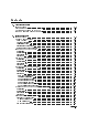
PERFORMANCE TEST RECORD Agilent Technologies 4291B RF Impedance/Material Analyzer Test Date Temperature Humidity Tested by: Serial No. Mainframe Test Station Norm-Temp High-Z Head Norm-Temp Low-Z Head High-Temp High-Z Head High-Temp Low-Z Head Frequency Accuracy Test Without Option 1D5 Frequency Test Limit 1 GHz Test Result 6 10.0 kHz Measurement Uncertainty 62.3 kHz kHz With Option 1D5 Frequency Test Limit 1 GHz Test Result 6 1.00 kHz Measurement Uncertainty kHz 60.
Norm-Temp Low-Impedance Test Head (Option 012) Osc Level Frequency Test Limit 019 dBm 013 dBm 07 dBm 1 dBm 7 dBm 1 MHz 10 MHz 100 MHz 1.8 GHz 1 GHz Test Result 63.00 dB 63.03 dB 63.33 dB 68.00 dB 65.33 dB Measurement Uncertainty dB dB dB dB dB 60.18 dB 60.19 dB 60.20 dB 60.19 dB 60.
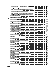
High-Temp Low-Impedance Test Head (Option 014) Osc Level Frequency Test Limit 019 dBm 019 dBm 019 dBm 019 dBm 019 dBm 019 dBm 019 dBm 019 dBm 013 dBm 07 dBm 07 dBm 07 dBm 07 dBm 07 dBm 07 dBm 07 dBm 07 dBm 07 dBm 07 dBm 07 dBm 07 dBm 1 dBm 1 dBm 2-22 Performance Tests 1 MHz 15 MHz 200 MHz 300 MHz 500 MHz 800 MHz 1.2 GHz 1.5 GHz 10 MHz 1 MHz 10 MHz 15 MHz 100 MHz 200 MHz 300 MHz 500 MHz 800 MHz 1 GHz 1.2 GHz 1.5 GHz 1.8 GHz 1 MHz 1 GHz 65.00 dB 65.07 dB 65.89 dB 66.33 dB 67.22 dB 68.56 dB 610.
Measurement Accuracy Test Norm-Temp High-Impedance Test Head Test Head: Standard: Osc Level: Norm-Temp High-Z Open 400 mV Frequency Measurement Parameter 1 MHz 10 MHz 100 MHz 200 MHz 300 MHz 500 MHz 600 MHz 800 MHz 1 GHz 1.3 GHz 1.6 GHz 1.8 GHz Test Head: Standard: Osc Level: jYj jYj jYj jYj jYj jYj jYj jYj jYj jYj jYj jYj Test Limit S S S S mS mS mS mS mS mS mS mS Test Result 62.12 S 63.24 S 614.4 S 628.4 S 641.8 S 669.1 S 697.
Test Head: Standard: Osc Level: Norm-Temp High-Z Short 400 mV Frequency Measurement Calibration Test Limit Parameter Value jZj jZj jZj jZj jZj jZj jZj jZj jZj jZj jZj jZj 1 MHz 10 MHz 100 MHz 200 MHz 300 MHz 500 MHz 600 MHz 800 MHz 1 GHz 1.3 GHz 1.6 GHz 1.8 GHz Test Head: Standard: Osc Level: 0.00 m 0.00 m 0.00 m 0.00 m 0.00 m 0.00 m 0.00 m 0.00 m 0.00 m 0.00 m 0.00 m 0.00 m 6101 m 6105 m 6150 m 6200 m 6250 m 6350 m 6400 m 6500 m 6600 m 6750 m 6900 m 61.
Test Head: Standard: Osc Level: Norm-Temp High-Z 50 400 mV Frequency Measurement Parameter 1 MHz 1 MHz 10 MHz 10 MHz 100 MHz 100 MHz 200 MHz 200 MHz 300 MHz 300 MHz 500 MHz 500 MHz 600 MHz 600 MHz 800 MHz 800 MHz 1 GHz 1 GHz 1.3 GHz 1.3 GHz 1.6 GHz 1.6 GHz 1.8 GHz 1.8 GHz jZj jZj jZj jZj jZj jZj jZj jZj jZj jZj jZj jZj Calibration Value mrad mrad mrad mrad mrad mrad mrad mrad mrad mrad mrad mrad Test Limit 6418 m 68.37 mrad 6425 m 68.
Test Head: Standard: Osc Level: Norm-Temp High-Z 50 41 mV Frequency Measurement Parameter 1 MHz 1 MHz 10 MHz 10 MHz 100 MHz 100 MHz 200 MHz 200 MHz 300 MHz 300 MHz 500 MHz 500 MHz 600 MHz 600 MHz 800 MHz 800 MHz 1 GHz 1 GHz 1.3 GHz 1.3 GHz 1.6 GHz 1.6 GHz 1.8 GHz 1.8 GHz 2-26 jZj jZj jZj jZj jZj jZj jZj jZj jZj jZj jZj jZj Performance Tests Calibration Value mrad mrad mrad mrad mrad mrad mrad mrad mrad mrad mrad mrad Test Limit 6451 m 69.
Test Head: Standard: Osc Level: Norm-Temp High-Z 10 cm Airline with Open 400 mV Frequency Measurement Parameter 1 MHz 1 MHz 10 MHz 10 MHz 100 MHz 100 MHz 200 MHz 200 MHz 300 MHz 300 MHz 500 MHz 500 MHz 600 MHz 600 MHz 800 MHz 800 MHz 1 GHz 1 GHz 1.6 GHz 1.6 GHz 1.8 GHz 1.8 GHz jZj jZj jZj jZj jZj jZj jZj jZj jZj jZj jZj Calibration Value Test Limit k rad k rad rad rad rad rad rad rad rad rad rad 61.13 k 651.8 mrad 627.5 612.6 mrad 62.22 610.
Test Head: Standard: Osc Level: Norm-Temp High-Z 10 cm Airline with Open 41 mV Frequency Measurement Parameter 1 MHz 1 MHz 10 MHz 10 MHz 100 MHz 100 MHz 200 MHz 200 MHz 300 MHz 300 MHz 500 MHz 500 MHz 600 MHz 600 MHz 800 MHz 800 MHz 1 GHz 1 GHz 1.6 GHz 1.6 GHz 1.8 GHz 1.8 GHz 2-28 jZj jZj jZj jZj jZj jZj jZj jZj jZj jZj jZj Performance Tests Calibration Value Test Limit k rad k rad rad rad rad rad rad rad rad rad rad 69.69 k 6444 mrad 6113 651.
Test Head: Standard: Osc Level: Norm-Temp High-Z 10 cm Airline with Short 400 mV Frequency Measurement Parameter 1 MHz 1 MHz 10 MHz 10 MHz 100 MHz 100 MHz 200 MHz 200 MHz 300 MHz 300 MHz 500 MHz 500 MHz 600 MHz 600 MHz 1 GHz 1 GHz 1.3 GHz 1.3 GHz 1.6 GHz 1.6 GHz 1.8 GHz 1.8 GHz jZj jZj jZj jZj jZj jZj jZj jZj jZj jZj jZj Calibration Value Test Limit m rad rad rad rad rad rad rad rad rad rad rad 6101 m 6893 mrad 6111 m 6104 mrad 6216 m 620.
Test Head: Standard: Osc Level: Norm-Temp High-Z 10 cm Airline with Short 41 mV Frequency Measurement Parameter 1 MHz 1 MHz 10 MHz 10 MHz 100 MHz 100 MHz 200 MHz 200 MHz 300 MHz 300 MHz 500 MHz 500 MHz 600 MHz 600 MHz 1 GHz 1 GHz 1.3 GHz 1.3 GHz 1.6 GHz 1.6 GHz 1.8 GHz 1.
Norm-Temp Low-Impedance Test Head (Option 012) Test Head: Standard: Osc Level: Norm-Temp Low-Z Open 400 mV Frequency Measurement Parameter 1 MHz 10 MHz 100 MHz 200 MHz 300 MHz 500 MHz 600 MHz 800 MHz 1 GHz 1.3 GHz 1.6 GHz 1.8 GHz Test Head: Standard: Osc Level: jYj jYj jYj jYj jYj jYj jYj jYj jYj jYj jYj jYj Test Limit S S S S mS mS mS mS mS mS mS mS Test Result 630.1 S 631.2 S 642.4 S 656.4 S 669.7 S 696.
Test Head: Standard: Osc Level: Norm-Temp Low-Z Short 400 mV Frequency Measurement Calibration Test Limit Parameter Value jZj jZj jZj jZj jZj jZj jZj jZj jZj jZj jZj jZj 1 MHz 10 MHz 100 MHz 200 MHz 300 MHz 500 MHz 600 MHz 800 MHz 1 GHz 1.3 GHz 1.6 GHz 1.8 GHz Test Head: Standard: Osc Level: 0.00 m 0.00 m 0.00 m 0.00 m 0.00 m 0.00 m 0.00 m 0.00 m 0.00 m 0.00 m 0.00 m 0.00 m 610.5 m 615.0 m 660.
Test Head: Standard: Osc Level: Norm-Temp Low-Z 50 400 mV Frequency Measurement Parameter 1 MHz 1 MHz 10 MHz 10 MHz 100 MHz 100 MHz 200 MHz 200 MHz 300 MHz 300 MHz 500 MHz 500 MHz 600 MHz 600 MHz 800 MHz 800 MHz 1 GHz 1 GHz 1.3 GHz 1.3 GHz 1.6 GHz 1.6 GHz 1.8 GHz 1.8 GHz jZj jZj jZj jZj jZj jZj jZj jZj jZj jZj jZj jZj Calibration Value mrad mrad mrad mrad mrad mrad mrad mrad mrad mrad mrad mrad Test Limit 6396 m 67.92 mrad 6403 m 68.
Test Head: Standard: Osc Level: Norm-Temp Low-Z 50 41 mV Frequency Measurement Parameter 1 MHz 1 MHz 10 MHz 10 MHz 100 MHz 100 MHz 200 MHz 200 MHz 300 MHz 300 MHz 500 MHz 500 MHz 600 MHz 600 MHz 800 MHz 800 MHz 1 GHz 1 GHz 1.3 GHz 1.3 GHz 1.6 GHz 1.6 GHz 1.8 GHz 1.8 GHz 2-34 jZj jZj jZj jZj jZj jZj jZj jZj jZj jZj jZj jZj Performance Tests Calibration Value mrad mrad mrad mrad mrad mrad mrad mrad mrad mrad mrad mrad Test Limit 6426 m 68.
Test Head: Standard: Osc Level: Norm-Temp Low-Z 10 cm Airline with Open 400 mV Frequency Measurement Parameter 1 MHz 1 MHz 10 MHz 10 MHz 100 MHz 100 MHz 200 MHz 200 MHz 300 MHz 300 MHz 500 MHz 500 MHz 600 MHz 600 MHz 800 MHz 800 MHz 1 GHz 1 GHz 1.6 GHz 1.6 GHz 1.8 GHz 1.8 GHz jZj jZj jZj jZj jZj jZj jZj jZj jZj jZj jZj Calibration Value Test Limit k rad k rad rad rad rad rad rad rad rad rad rad 614.4 k 6662 mrad 6161 673.6 mrad 63.19 614.
Test Head: Standard: Osc Level: Norm-Temp Low-Z 10 cm Airline with Open 41 mV Frequency Measurement Parameter 1 MHz 1 MHz 10 MHz 10 MHz 100 MHz 100 MHz 200 MHz 200 MHz 300 MHz 300 MHz 500 MHz 500 MHz 600 MHz 600 MHz 800 MHz 800 MHz 1 GHz 1 GHz 1.6 GHz 1.6 GHz 1.8 GHz 1.8 GHz 2-36 jZj jZj jZj jZj jZj jZj jZj jZj jZj jZj jZj Performance Tests Calibration Value Test Limit k rad k rad rad rad rad rad rad rad rad rad rad 614.4 k 6662 mrad 6161 673.
Test Head: Standard: Osc Level: Norm-Temp Low-Z 10 cm Airline with Short 400 mV Frequency Measurement Parameter 1 MHz 1 MHz 10 MHz 10 MHz 100 MHz 100 MHz 200 MHz 200 MHz 300 MHz 300 MHz 500 MHz 500 MHz 600 MHz 600 MHz 1 GHz 1 GHz 1.3 GHz 1.3 GHz 1.6 GHz 1.6 GHz 1.8 GHz 1.8 GHz jZj jZj jZj jZj jZj jZj jZj jZj jZj jZj jZj Calibration Value Test Limit m rad rad rad rad rad rad rad rad rad rad rad 611.2 m 698.7 mrad 621.5 m 620.0 mrad 6139 m 613.
Test Head: Standard: Osc Level: Norm-Temp Low-Z 10 cm Airline with Short 41 mV Frequency Measurement Parameter 1 MHz 1 MHz 10 MHz 10 MHz 100 MHz 100 MHz 200 MHz 200 MHz 300 MHz 300 MHz 500 MHz 500 MHz 600 MHz 600 MHz 1 GHz 1 GHz 1.3 GHz 1.3 GHz 1.6 GHz 1.6 GHz 1.8 GHz 1.8 GHz 2-38 jZj jZj jZj jZj jZj jZj jZj jZj jZj jZj jZj Performance Tests Calibration Value Test Limit m rad rad rad rad rad rad rad rad rad rad rad 651.2 m 6452 mrad 661.5 m 657.
High-Temp High-Impedance Test Head (Option 013) Test Head: Standard: Osc Level: High-Temp High-Z Open 250 mV Frequency Measurement Parameter 1 MHz 10 MHz 100 MHz 200 MHz 300 MHz 500 MHz 600 MHz 800 MHz 1 GHz 1.3 GHz 1.6 GHz 1.8 GHz Test Head: Standard: Osc Level: jYj jYj jYj jYj jYj jYj jYj jYj jYj jYj jYj jYj Test Limit S S S S mS mS mS mS mS mS mS mS Test Result 610.2 S 612.2 S 632.4 S 656.5 S 680.
Test Head: Standard: Osc Level: High-Temp High-Z Short 250 mV Frequency Measurement Calibration Test Limit Parameter Value jZj jZj jZj jZj jZj jZj jZj jZj jZj jZj jZj jZj 1 MHz 10 MHz 100 MHz 200 MHz 300 MHz 500 MHz 600 MHz 800 MHz 1 GHz 1.3 GHz 1.6 GHz 1.8 GHz Test Head: Standard: Osc Level: 0.00 m 0.00 m 0.00 m 0.00 m 0.00 m 0.00 m 0.00 m 0.00 m 0.00 m 0.00 m 0.00 m 0.00 m 6101 m 6110 m 6200 m 6300 m 6400 m 6600 m 6700 m 6900 m 61.10 61.40 61.70 61.
Test Head: Standard: Osc Level: High-Temp High-Z 50 250 mV Frequency Measurement Parameter 1 MHz 1 MHz 10 MHz 10 MHz 100 MHz 100 MHz 200 MHz 200 MHz 300 MHz 300 MHz 500 MHz 500 MHz 600 MHz 600 MHz 800 MHz 800 MHz 1 GHz 1 GHz 1.3 GHz 1.3 GHz 1.6 GHz 1.6 GHz 1.8 GHz 1.8 GHz jZj jZj jZj jZj jZj jZj jZj jZj jZj jZj jZj jZj Calibration Value mrad mrad mrad mrad mrad mrad mrad mrad mrad mrad mrad mrad Test Limit 6427 m 68.53 mrad 6440 m 68.
Test Head: Standard: Osc Level: High-Temp High-Z 50 41 mV Frequency Measurement Parameter 1 MHz 1 MHz 10 MHz 10 MHz 100 MHz 100 MHz 200 MHz 200 MHz 300 MHz 300 MHz 500 MHz 500 MHz 600 MHz 600 MHz 800 MHz 800 MHz 1 GHz 1 GHz 1.3 GHz 1.3 GHz 1.6 GHz 1.6 GHz 1.8 GHz 1.8 GHz 2-42 jZj jZj jZj jZj jZj jZj jZj jZj jZj jZj jZj jZj Performance Tests Calibration Value mrad mrad mrad mrad mrad mrad mrad mrad mrad mrad mrad mrad Test Limit 6452 m 69.
Test Head: Standard: Osc Level: High-Temp High-Z 10 cm Airline with Open 250 mV Frequency Measurement Parameter 1 MHz 1 MHz 10 MHz 10 MHz 100 MHz 100 MHz 200 MHz 200 MHz 300 MHz 300 MHz 500 MHz 500 MHz 600 MHz 600 MHz 800 MHz 800 MHz 1 GHz 1 GHz 1.6 GHz 1.6 GHz 1.8 GHz 1.8 GHz jZj jZj jZj jZj jZj jZj jZj jZj jZj jZj jZj Calibration Value Test Limit k rad k rad rad rad rad rad rad rad rad rad rad 64.98 k 6228 mrad 670.3 632.2 mrad 62.86 613.
Test Head: Standard: Osc Level: High-Temp High-Z 10 cm Airline with Open 41 mV Frequency Measurement Parameter 1 MHz 1 MHz 10 MHz 10 MHz 100 MHz 100 MHz 200 MHz 200 MHz 300 MHz 300 MHz 500 MHz 500 MHz 600 MHz 600 MHz 800 MHz 800 MHz 1 GHz 1 GHz 1.6 GHz 1.6 GHz 1.8 GHz 1.8 GHz 2-44 jZj jZj jZj jZj jZj jZj jZj jZj jZj jZj jZj Performance Tests Calibration Value Test Limit k rad k rad rad rad rad rad rad rad rad rad rad 69.74 k 6447 mrad 6118 654.
Test Head: Standard: Osc Level: High-Temp High-Z 10 cm Airline with Short 250 mV Frequency Measurement Parameter 1 MHz 1 MHz 10 MHz 10 MHz 100 MHz 100 MHz 200 MHz 200 MHz 300 MHz 300 MHz 500 MHz 500 MHz 600 MHz 600 MHz 1 GHz 1 GHz 1.3 GHz 1.3 GHz 1.6 GHz 1.6 GHz 1.8 GHz 1.8 GHz jZj jZj jZj jZj jZj jZj jZj jZj jZj jZj jZj Calibration Value Test Limit m rad rad rad rad rad rad rad rad rad rad rad 6102 m 6897 mrad 6116 m 6109 mrad 6268 m 625.
Test Head: Standard: Osc Level: High-Temp High-Z 10 cm Airline with Short 41 mV Frequency Measurement Parameter 1 MHz 1 MHz 10 MHz 10 MHz 100 MHz 100 MHz 200 MHz 200 MHz 300 MHz 300 MHz 500 MHz 500 MHz 600 MHz 600 MHz 1 GHz 1 GHz 1.3 GHz 1.3 GHz 1.6 GHz 1.6 GHz 1.8 GHz 1.
High-Temp Low-Impedance Test Head (Option 014) Test Head: Standard: Osc Level: High-Temp Low-Z Open 250 mV Frequency Measurement Parameter 1 MHz 10 MHz 100 MHz 200 MHz 300 MHz 500 MHz 600 MHz 800 MHz 1 GHz 1.3 GHz 1.6 GHz 1.8 GHz Test Head: Standard: Osc Level: jYj jYj jYj jYj jYj jYj jYj jYj jYj jYj jYj jYj Test Limit S S S S mS mS mS mS mS mS mS mS Test Result 630.2 S 632.2 S 652.4 S 676.4 S 699.
Test Head: Standard: Osc Level: High-Temp Low-Z Short 250 mV Frequency Measurement Calibration Test Limit Parameter Value jZj jZj jZj jZj jZj jZj jZj jZj jZj jZj jZj jZj 1 MHz 10 MHz 100 MHz 200 MHz 300 MHz 500 MHz 600 MHz 800 MHz 1 GHz 1.3 GHz 1.6 GHz 1.8 GHz Test Head: Standard: Osc Level: 0.00 m 0.00 m 0.00 m 0.00 m 0.00 m 0.00 m 0.00 m 0.00 m 0.00 m 0.00 m 0.00 m 0.00 m 631.0 m 640.0 m 6130 m 6230 m 6330 m 6530 m 6630 m 6830 m 61.03 61.33 61.63 61.
Test Head: Standard: Osc Level: High-Temp Low-Z 50 250 mV Frequency Measurement Parameter 1 MHz 1 MHz 10 MHz 10 MHz 100 MHz 100 MHz 200 MHz 200 MHz 300 MHz 300 MHz 500 MHz 500 MHz 600 MHz 600 MHz 800 MHz 800 MHz 1 GHz 1 GHz 1.3 GHz 1.3 GHz 1.6 GHz 1.6 GHz 1.8 GHz 1.8 GHz jZj jZj jZj jZj jZj jZj jZj jZj jZj jZj jZj jZj Calibration Value mrad mrad mrad mrad mrad mrad mrad mrad mrad mrad mrad mrad Test Limit 6407 m 68.13 mrad 6420 m 68.
Test Head: Standard: Osc Level: High-Temp Low-Z 50 41 mV Frequency Measurement Parameter 1 MHz 1 MHz 10 MHz 10 MHz 100 MHz 100 MHz 200 MHz 200 MHz 300 MHz 300 MHz 500 MHz 500 MHz 600 MHz 600 MHz 800 MHz 800 MHz 1 GHz 1 GHz 1.3 GHz 1.3 GHz 1.6 GHz 1.6 GHz 1.8 GHz 1.8 GHz 2-50 jZj jZj jZj jZj jZj jZj jZj jZj jZj jZj jZj jZj Performance Tests Calibration Value mrad mrad mrad mrad mrad mrad mrad mrad mrad mrad mrad mrad Test Limit 6427 m 68.
Test Head: Standard: Osc Level: High-Temp Low-Z 10 cm Airline with Open 250 mV Frequency Measurement Parameter 1 MHz 1 MHz 10 MHz 10 MHz 100 MHz 100 MHz 200 MHz 200 MHz 300 MHz 300 MHz 500 MHz 500 MHz 600 MHz 600 MHz 800 MHz 800 MHz 1 GHz 1 GHz 1.6 GHz 1.6 GHz 1.8 GHz 1.8 GHz jZj jZj jZj jZj jZj jZj jZj jZj jZj jZj jZj Calibration Value Test Limit k rad k rad rad rad rad rad rad rad rad rad rad 614.5 k 6665 mrad 6165 675.8 mrad 63.71 617.
Test Head: Standard: Osc Level: High-Temp Low-Z 10 cm Airline with Open 41 mV Frequency Measurement Parameter 1 MHz 1 MHz 10 MHz 10 MHz 100 MHz 100 MHz 200 MHz 200 MHz 300 MHz 300 MHz 500 MHz 500 MHz 600 MHz 600 MHz 800 MHz 800 MHz 1 GHz 1 GHz 1.6 GHz 1.6 GHz 1.8 GHz 1.8 GHz 2-52 jZj jZj jZj jZj jZj jZj jZj jZj jZj jZj jZj Performance Tests Calibration Value Test Limit k rad k rad rad rad rad rad rad rad rad rad rad 614.5 k 6665 mrad 6165 675.
Test Head: Standard: Osc Level: High-Temp Low-Z 10 cm Airline with Short 250 mV Frequency Measurement Parameter 1 MHz 1 MHz 10 MHz 10 MHz 100 MHz 100 MHz 200 MHz 200 MHz 300 MHz 300 MHz 500 MHz 500 MHz 600 MHz 600 MHz 1 GHz 1 GHz 1.3 GHz 1.3 GHz 1.6 GHz 1.6 GHz 1.8 GHz 1.8 GHz jZj jZj jZj jZj jZj jZj jZj jZj jZj jZj jZj Calibration Value Test Limit m rad rad rad rad rad rad rad rad rad rad rad 631.7 m 6280 mrad 646.5 m 643.3 mrad 6200 m 618.
Test Head: Standard: Osc Level: High-Temp Low-Z 10 cm Airline with Short 41 mV Frequency Measurement Parameter 1 MHz 1 MHz 10 MHz 10 MHz 100 MHz 100 MHz 200 MHz 200 MHz 300 MHz 300 MHz 500 MHz 500 MHz 600 MHz 600 MHz 1 GHz 1 GHz 1.3 GHz 1.3 GHz 1.6 GHz 1.6 GHz 1.8 GHz 1.8 GHz 2-54 jZj jZj jZj jZj jZj jZj jZj jZj jZj jZj jZj Performance Tests Calibration Value Test Limit m rad rad rad rad rad rad rad rad rad rad rad 651.7 m 6456 mrad 666.5 m 662.
DC Bias Accuracy Test Bias Level Test Limit 0V 4V 10 V 40 V 04 V 010 V 040 V 0A 20 A 1 mA 10 mA 100 mA 020 A 01 mA 010 mA 0100 mA 64.00 mV 68.00 mV 614.0 mV 644.0 mV 68.00 mV 614.0 mV 644.0 mV 630.0 A 630.1 A 635.0 A 680.0 A 6530 A 630.1 A 635.0 A 680.0 A 6530 A Test Result Measurement Uncertainty mV mV mV mV mV mV mV A A A A A A A A A 60.02 mV 60.07 mV 60.1 mV 61.1 mV 60.07 mV 60.1 mV 61.1 mV 60.0 A 60.0 A 60.1 A 60.9 A 618 A 60.0 A 60.1 A 60.
3 Adjustments and Correction Constants INTRODUCTION This chapter describes the Adjustments and Correction Constants procedures required to ensure that the 4291B RF Impedance/Material Analyzer is within its speci cations. These adjustments should be performed along with periodic maintenance to keep the analyzer in optimum operating condition. The recommended calibration period is 12 months.
REQUIRED EQUIPMENT Table 1-1 lists the equipment required to perform the Adjustments and the Correction Constants procedures described in this chapter. Use only calibrated test equipment when adjusting the analyzer. If the recommended test equipment is not available, equipment whose speci cations are equal to, or surpasses those of the recommended test equipment may be used.
UPDATING Correction Constants USING THE ADJUSTMENTS PROGRAM This section provides general information on how to update the Correction Constants using the adjustments program. Adjustments Program The adjustments program is provided on one double-sided diskette. The diskette's Agilent part number is 04291-65003.
Controller Requirement The following controller system is required to run the adjustments program: Controller HP 9000 Series 200/300 computer Excluding HP 9826A computers Must have inverse video capability At least 4 M bytes of RAM Mass Storage At least one 3.5 inch GPIB Flexible Disk Drive HFS formatted hard disk system or SRM system are supported. The controller must be equipped with HP BASIC versions between 5.1 and 5.13, and the language extension les listed in Table 3-1.
Updating Correction Constants Correction Constants are updated using the following procedure: 1. Connect the equipment as shown in Figure 3-1 Note Figure 3-1. Updating Correction Constants Setup Steps 2 to 5 are used to select the equipment and to set their GPIB addresses. When you perform the Adjustments Program the rst time, perform these steps to select the equipment and the GPIB address. After that, perform the \TE A4291B" program only when you want to change the equipment or the GPIB address. 2.
40 MHz REFERENCE OSCILLATOR FREQUENCY ADJUSTMENT The purpose of this procedure is to adjust the 40 MHz reference oscillator frequency.
Figure 3-3. 40 MHz Reference Oscillator Frequency Adjustment Location 2. Set the frequency counter as follows: Input Impedance 50 Frequency Range 10 Hz - 500 MHz 3. Adjust A5 \40 MHz FREQ ADJ" until the frequency counter reading is within 20 MHz 6 20 Hz. The adjustment location is shown in Figure 3-3.
520 MHz LEVEL ADJUSTMENT The purpose of this procedure is to adjust the 520 MHz output level.
Figure 3-5. 520 MHz Level Adjustment Setup 4. Set the spectrum analyzer as follows: CENTER Frequency 520 MHz SPAN 1 MHz RBW 100 kHz 5. Turn the 4291B analyzer ON. 6. Adjust A5 \520 MHz LEVEL ADJ" until the spectrum analyzer reading for the 520 MHz signal level is within 015 6 0.2 dBm. The adjustment location is shown in Figure 3-4. 7. Turn the 4291B analyzer OFF. 8. Reconnect the \J" cable to the A5 \520 MHz OUT" connector.
COMB GENERATOR ADJUSTMENT The purpose of this procedure is to adjust the comb generator output level.
Figure 3-7. Comb Generator Adjustment Location 3. Set the spectrum analyzer as follows: Start Frequency Stop Frequency RBW Reference Level Scale 400 MHz 1 GHz 1 MHz 0 20 dBm 5 dB/div 4. Turn the 4291B analyzer ON. 5. Adjust A5 \COMB DC BIAS ADJ" until the spectrum analyzer display indicates the following: 720 MHz Signal Level between 046 and 037 dBm 480 MHz to 920 MHz Flatness < 8 dBm 480 MHz to 920 MHz Signal Level > 051 dBm The adjustment location is shown in Figure 3-7.
Figure 3-8.
STEP PRETUNE CORRECTION CONSTANTS The purpose of this procedure is to generate the correction constants that are used to pretune the step loop oscillator. Required Equipment None Procedure 1. Run the adjustment program and display the main menu (see \UPDATING Correction Constants USING THE ADJUSTMENTS PROGRAM"). 2. Choose the Step Pretune Correction Constants. 3. Follow the adjustment program instructions to update the correction constants.
SECOND LOCAL PLL LOCK ADJUSTMENT The purpose of this procedure is to lock the second local Phase Lock Loop (PLL).
Figure 3-10. Second Local PLL Adjustment Setup 4. Set the spectrum analyzer as follows: Center Frequency 2.08 GHz Span 400 MHz RBW 1 MHz 5. Turn the 4291B analyzer ON. 6. Press the following keys to execute adjustment Test No.37: 4PRESET5, 4SYSTEM5, NNNNNNNNNNNNNNNNNNNNNNNNNNNNNNNNNNNNNN NNNNNNNNNNNNNNNNN NNNNNNNNNNNNNNNNNNNNNNNNNNNNNNNNNNNNNN SERVICE MENU , TESTS , 435, 475, 4x15, EXECUTE TEST 7. Adjust A3A2 \Second Local Adj" until 2.
SOURCE VCXO ADJUSTMENT The purpose of this procedure is to optimize the source VCXO oscillation. Required Equipment None Procedure 1. Do not connect anything to the analyzer mainframe front terminals. 2. Press the following keys to execute adjustment Test No.39: 4PRESET5, 4SYSTEM5, NNNNNNNNNNNNNNNNNNNNNNNNNNNNNNNNNNNNNN NNNNNNNNNNNNNNNNNNNNNNNNNNNNNNNNNNNNNN NNNNNNNNNNNNNNNNN SERVICE MENU , TESTS , 435, 495, 4x15, EXECUTE TEST 3.
THIRD LOCAL VCXO ADJUSTMENT The purpose of this procedure is to optimize the source VCXO oscillation. Required Equipment None Procedure 1. 2. 3. 4. Turn the analyzer OFF. To gain access to the adjustment component, remove the side panel on the control keys side. Do not connect anything to the analyzer mainframe front terminals. Press the following keys to execute adjustment Test No.
SOURCE MIXER LOCAL LEAKAGE ADJUSTMENT The purpose of this procedure is to minimize the source mixer local leakage.
4. Adjust the local leakage adjustments until the spectrum analyzer reading of the 78.58 MHz signal level is smaller than 040 dBm. Then press CONT to complete the adjustment. The adjustment locations are shown in Figure 3-14. NNNNNNNNNNNNNN Note Carefully rotate the local leakage adjustments so that the adjustments are not misadjusted by much. It would be very di cult to recover from a large misadjustment. Figure 3-14.
OSC LEVEL CORRECTION CONSTANTS The purpose of this procedure is to obtain the correction constants that correct the OSC signal linearity and atness.
HOLD STEP ADJUSTMENT The purpose of this procedure is to minimize the hold step of the A6 receiver sample and hold output. Required Equipment None Procedure 1. 2. 3. 4. 5. Turn the analyzer OFF. To gain access to the adjustment component, remove the side panel on the control keys side. Do not connect anything to the analyzer mainframe front terminals. Turn the analyzer ON. Press the following keys to execute adjustment Test No.
BAND PASS FILTER ADJUSTMENT The purpose of this procedure is to optimize the A6 receiver IF band pass lter. Required Equipment Type-N Cable, 61 cm : : : : : : : : : : : : : : : : : : : : : : : : : : : : : : : : : : : : : : : : : : : : : : : : : : 11500B or part of 11851B Procedure 1. Turn the analyzer OFF. 2. To gain access to the adjustment component, remove the side panel on the control keys side. 3. Connect the equipment as shown in Figure 3-17. Figure 3-17. Band Pass Filter Adjustment Setup 4.
Figure 3-18.
DC BIAS LEVEL CORRECTION CONSTANTS (OPTION 001 ONLY) The purpose of this procedure is to obtain the correction constants that correct the DC bias voltage and current level.
10 MHz REFERENCE OSCILLATOR FREQUENCY ADJUSTMENT (OPTION 1D5 ONLY) The purpose of this procedure is to adjust the 10 MHz high stability reference oscillator (Option 1D5) frequency.
4. Connect a BNC(m)-BNC(m) cable between the \EXT REF" input connector and the \REF OVEN" connector on the analyzer rear panel. Then connect the equipment as shown in Figure 3-21. Figure 3-21. 10 MHz Reference Oscillator Frequency Adjustment Setup 5. Press 4 5 Preset to initialize the analyzer. Then set the analyzer controls as follows: Control Settings Frequency Span: 0 Hz Center Frequency: 1.8 GHz Source Power: 033 dBm Key Strokes 4Span5, 405, 4x15 4Center5, 415, 4.
4 Overall Troubleshooting This chapter consists of the following sections: Troubleshooting Summary Inspect the Power ON Sequence Verify Functional Groups Troubleshooting the GPIB System The Troubleshooting Summary outlines how to troubleshoot the 4291B using the troubleshooting ow diagram. The Inspect the Power ON Sequence begins the troubleshooting procedures by inspecting the power on sequence.
TROUBLESHOOTING SUMMARY The troubleshooting strategy of this manual is based on a veri cation (rather than symptomatic) approach. Veri cation procedures and the resulting corrective actions are given in the manual. By following these directions, you will determine the faulty assembly that must be replaced. Figure 4-1 shows the overall troubleshooting ow.
Figure 4-1.
INSPECT THE POWER ON SEQUENCE This section begins the troubleshooting procedures by inspecting the power on sequence. Check the Fan Turn the analyzer power on. Inspect the fan on the rear panel. The fan should be rotating and audible. In case of unexpected results, check the AC line power to the analyzer. Check the fuse (the rating is listed on the rear panel). Check the line voltage setting. To set the line voltage, see the Power Requirements in Appendix B.
Check Error Message Turn the analyzer power on, and inspect the display. No error message should be displayed. If one of the error messages listed below is displayed, follow the related instructions. For any other message, see the Error Messages in the Messages appendix. Error Messages Instruction POWER ON TEST FAILED EEPROM CHECK SUM ERROR Svc (Status Annotation) POWER FAILED ON - - - POWER FAILED ON PostRegHot PHASE LOCK LOOP UNLOCKED This indicates the power on self-test failed.
Table 4-1. Troubleshooting Information for Internal Test Failure Troubleshooting Information First Failed Test Test No. 1 1 4 A1 CPU A2 POST REGULATOR 5 A6 A/D CONVERTER 6 A5 REFERENCE OSC 7 A5 FRACTIONAL N 8 A5 STEP OSC 9 A4A1 1ST LO OSC 10 A3A2 2ND LO OSC 11 A3A1 DIVIDER 12 A6 3RD LO OSC 13 A3A1 SOURCE OSC 14 A6 SEQUENCER 15 16 SOURCE LEVEL DC BIAS Replace A1 CPU. Continue with the A2 POST REGULATOR Test Fail section. The A6 receiver IF is the most probable faulty board.
VERIFY FUNCTIONAL GROUPS This section provides faulty group isolation procedures. Source Test Verify the source group operation by performing following procedure. Test Equipment Frequency Counter : : : : : : : : : : : : : : : : : : : : : : : : : : : : : : : : : : : : : : : : : : : : : : : : : : : : : : : : : : : 5343A Option 001 Power meter : : : : : : : : : : : : : : : : : : : : : : : : : : : : : : : : : : : : : : : : : : : : : : : : : : : : : 436A Opt.
8. Con rm that the power meter reading is within the test limits shown in Table 4-2. Table 4-2. Source Test Settings Frequency Osc Level Test Limit 019 dBm 6 2 dB 013 dBm 6 2 dB 07 dBm 6 2 dB 7 dBm 6 2 dB 1 dBm 6 3 dB 1 MHz 10 MHz 100 MHz 1 GHz 1.8 GHz 9. Perform the test for all settings listed in Table 4-2. If the test fails, perform the OSC level correction constants according to Chapter 3. If the test still fails, go to Chapter 7. If the test passes, continue with the next step.
Receiver Test Verify the receiver operation by performing following procedure. Test Equipment Type-N Cable, 61 cm : : : : : : : : : : : : : : : : : : : : : : : : : : : : : : : : : : : : : : : : : : : : : : : : : : 11500B or part of 11851B Procedure 1. 2. 3. 4. Verify that nothing is connected to the front panel of the analyzer mainframe. Turn the analyzer power on. 5 to initialize the analyzer.
Transducer Test Verify the transducer operation by performing following procedures. Test Equipment Calibration Kit : : : : : : : : : : : : : : : : : : : : : : : : : : : : : : : : : : : : : : : : : : : : : : : : : : : : : : : 4291B furnished accessory Procedure Note The 4291B has the following four test heads (including the optional test heads). Perform this test for all the available test heads.
Table 4-3. Test Head Tests List Test Number Test Name 30 HI Z HEAD 31 LO Z HEAD 32 HI TEMP HI Z HEAD 33 HI TEMP LO Z TEST NNNNNNNNNNNNNNNNNNNNNNNNNNNNNNNNNNNNNN 5. Press EXECUTE TEST and perform the test according to the displayed instructions. If the test fails, go to Chapter 9. If the test passes, perform the test for the other available test heads in the same manner.
INSPECT THE REAR PANEL FUNCTION If the analyzer is operating unexpectedly after these checks are veri ed, continue with Digital Control Troubleshooting chapter. Check the GPIB Interface If the unexpected operations appear when controlling the analyzer with an external controller, perform the following checks to verify the problem is not with the controller. Compatibility, must be HP 9000 series 200/300, see the manuals of the controller and the BASIC system.
5 Power Supply Troubleshooting INTRODUCTION Use this procedure only if you have read Troubleshooting, and you believe the problem is in the power supply. The procedure is designed to let you identify the bad assembly within the power supply functional group in the shortest possible time. The power supply functional group consists of: A40 Pre-Regulator A50 DC-DC Converter A2 Post-Regulator All assemblies, however, are related to the power supply functional group because power is supplied to each assembly.
Figure 5-1.
START HERE 1. Check Error Messages Turn the analyzer power on. If one of error messages listed below appears on the display, follow the instruction of the displayed error message. If no error message is displayed, continue with Check the Fan is Rotating. Error Messages Instruction One or more of the A2 power supplies (+15 V, +8.5V, +5.3 V, +5 V, -5 V, -15 V) are displayed in - - - of the message. The displayed power supplies are shut down because of trouble on the A2 post-regulator.
If the A50 SHUTDOWN LED is o , check the cable connection between A40J2 and A2J4. If the connection is good, continue with FIND OUT WHY THE A50 SHUTDOWN LED IS ON in this chapter. If the A50 SHUTDOWN LED is on, continue with Check the A1 +5 VD LED in this procedure. Figure 5-2. A50 SHUTDOWN LED Location A50 SHUTDOWN LED The A50 SHUTDOWN LED turning o indicates some of A50 power supply is shut down by the A50 shutdown circuitry.
4. Check the A1 +5 VD LED a. Remove the analyzer's bottom cover. b. Turn the analyzer power on. c. Look at the +5 VD LED. Figure 5-3 shows the +5 VD LED location on A1 CPU. The LED is normally on. If the +5 VD LED is o , continue with TROUBLESHOOT +5 VD POWER SUPPLY in this chapter. If the +5 VD LED is on, the +5 VD power supply is veri ed with a 95% con dence level. Continue with Check Eight A2 LEDs in this procedure.
If the LEDs are correctly on, continue with Run the Internal Test 4: A2 POST REGULATOR. Figure 5-4. Eight A2 LED Locations 6. Run Internal Test 4: A2 POST REGULATOR Internal test 4: A2 POST REGULATOR veri es the A2 post-regulator. Perform the following procedure to check the A2 post-regulator. Internal test 4 is described in Internal Test 4: A2 POST REGULATOR. Note Internal test 4: A2 POST REGULATOR is a built-in diagnostic test.
Figure 5-5. Displayed Test Result If \PASS" is displayed, the power supply function group are working properly with a 95% con dence level. To con rm the last 5% uncertainty of the A2 power supplies, measure all A2 power supply voltages. See the MEASURE A2 POST-REGULATOR OUTPUT VOLTAGE at the end of this chapter. If \FAIL" is displayed, perform the following steps. a. Press RETURN , SERVICE MODES , BUS MEAS [ON] , DC BUS . Then the abbreviated faulty power supply is displayed on the LCD. b.
FIND OUT WHY THE FAN IS NOT ROTATING If the fan is not rotating, the problem may be in the A40 pre-regulator, the A50 DC-DC Converter, the A2 post-regulator, or the fan. 1. Check the Line Voltage, Selector Switch Setting, and Fuse Check the main power line cord, line fuse, and actual line voltage to see that they are all correct. Figure 5-6 shows how to remove the line fuse, using a small at-bladed screwdriver to pry o the fuse holder.
FIND OUT WHY THE A50 SHUTDOWN LED IS OFF Use this procedure when the fan is rotating. If the fan is not rotating, see the FIND OUT WHY THE FAN IS NOT ROTATING. If the fan is rotating, the A50 SHUTDOWN LED turning o indicates the A50 shutdown circuit is protecting the +5 VD power supply from the over voltage condition. The +5 VD power line may be shorted with one of power lines higher than +5 V.
5. Remove Assemblies a. Turn the analyzer power o . b. Remove the assemblies, A3, A4, A5, and A6. Don't remove the A2 post-regulator. c. Turn the analyzer power on. If the A50 SHUTDOWN LED is still o , the A2 post-regulator is probably faulty. Replace the A2 post-regulator. If the SHUTDOWN LED is still o after replacing the A2 post-regulator, inspect the A20 motherboard for soldering bridges and shorted traces on the FAN POWER and the FAN LOCK signal paths.
FIND OUT WHY THE A1 +5 VD LED IS NOT ON STEADILY If the +5 VD LED is not on steadily, the +5 VD line voltage is missing or is not steady enough to power the analyzer. The problem may be in the A40 pre-regulator, A50 DC-DC Converter, the A1 CPU, or any of assemblies obtaining power from +5 VD supply. 1. Check the A40 Pre-regulator a. b. c. d. Turn the analyzer power o . Disconnect the cable from A40J1. The A40J1 location is shown in Figure 5-7. Turn the analyzer power on.
If the voltmeter reading is within the limits, the A50 +5 VD power supply is veri ed. Turn the analyzer power o and reconnect the cable to the A50J3. Then continue with the next Disconnect Cables on the A1 CPU section. 3. Disconnect Cables on the A1 CPU a. Turn the analyzer power o . b. Disconnect cables from the A1 CPU's connectors, J10, J11 (if option 1C2 installed), J12, J13, J14, J16, and J17. The connector locations are shown in Figure 5-8 Figure 5-8. A1 CPU Connector Locations c.
4. Remove Assemblies a. Turn the analyzer power o . Remove the A3, A4, A5, and A6 assemblies. Do not remove the A2 post-regulator. b. Turn the analyzer power on. Look at the A1 +5 VD LED. If the LED is still o , replace the A2 post-regulator. If the +5 VD LED is still o after replacing the A2 post-regulator, inspect the A20 motherboard for soldering bridges and shorted traces on the +5 VD power line. If the LED goes on, the A2 post-regulator and the A20 motherboard are veri ed. Continue with the next step.
TROUBLESHOOT THE FAN AND THE A50 DC-DC CONVERTER Perform the following procedure to troubleshoot the fan and the A50 DC-DC Converter. 1. Troubleshoot the Fan a. b. c. d. Turn the analyzer power o . Disassemble the rear panel. Remove the fan power cable from the Motherboard A20J18. Connect a DC power supply, a 10 k resistance, and a oscilloscope to the fan power cable using appropriate wires as shown in Figure 5-9. Figure 5-9. Fan Troubleshooting Setup e. Turn the DC power supply on.
2. Troubleshoot the A50 DC-DC Converter Figure 5-10. A50 DC-DC Converter Troubleshooting Setup a. Turn the analyzer power o . b. Disconnect cables from the A50J2 and A50J3. The connector locations are shown in Figure 5-10 c. Connect the pulse generator to the A50J2 as shown in Figure 5-10. The pulse generator is used to feed the substitute of the FAN LOCK signal to the A50 DC-DC converter. This purposes not to shut down the A50 DC-DC converter. d. Turn the pulse generator power on.
Table 5-1. A50 Power Supplies Supply Connector Pin GND Connector Pin Range +5 VD A50J3 Pin 1, 2, and 3 A50J3 Pin 4, 5, and 6 +4.6 V to +5.7 V -18 V A50J2 Pin 1 A50J2 Pin 3 and 4 -14.0 V to -27.0 V +18 V A50J2 Pin 2 A50J2 Pin 3 and 4 14.0 V to 27.0 V +7.8 V A50J2 Pin 5 A50J2 Pin 3 and 4 7.0 V to 9.0 V -7.8 V A50J2 Pin 6 A50J2 Pin 3 and 4 -6.0 V to -12.0 V +24 V A50J2 Pin 8 A50J2 Pin 10 22.0 V to 27.
TROUBLESHOOT THE A2 POST-REGULATOR Use this procedure when the fan is rotating and the A50 SHUTDOWN LED turns on. If one or some of the A2 eight LEDs are not on steadily, the corresponding A2 power supply voltages, -15 V, -5 V, +5 V, +5.3 V, +15 VD, are missing or are not enough to power the analyzer. The problem may be in the A40 pre-regulator, the A50 DC-DC Converter, the A2 post-regulator, and any of assemblies obtaining the A2 post-regulator. 1.
Figure 5-11. A2 Output Voltage Measurement Setup e. Connect the pulse generator to the A2J4 as shown in Figure 5-11. f. Turn the pulse generator power on. Set the controls as follows: Wave Form Square Frequency Approximately 30 Hz Amplitude +7.8 V g. Turn the analyzer power on. h. Measure the A2 output voltages at the A2J3 pins using a voltmeter with a small probe. See Figure 5-11 and Table 5-2 for the power supplies, A2J3, and the limits.
Table 5-2. Power Supplies on A2 Post-Regulator Supply Connector Pin Range +22 V J3 Pin 8 19.8 V to 24.2 V +15 V(AUX) J3 Pin 4 13.5 V to 16.5 V +15 V J3 Pin 31 13.5 V to 16.5 V +8.5 V J3 Pin 25C 7.65 V to 9.35 V +5.3 V J3 Pin 25A 25B 4.77 V to 5.83 V +5 V J3 Pin 30 29 4.5 V to 5.5 V -5 V J3 Pin 28 -4.5 V to -5.5 V -12 V J3 Pin 5 -10.8 V to -13.2 V -15 V J3 Pin 27 -13.5 V to -16.5 V FAN POWER J3 Pin 8 19.2 V to 28.
Figure 5-12.
Figure 5-13.
Figure 5-14.
6 Digital Control Troubleshooting INTRODUCTION Use this procedure only if you have followed the procedures in the Troubleshooting chapter, and believe the problem to be in the digital control group. This procedure is designed to let you identify the bad assembly within the digital control group in the shortest possible time. Whenever an assembly is replaced in this procedure, refer to the Table of Related Service Procedures in the Post-Repair Procedures chapter in this manual.
Figure 6-1.
START HERE 1. Check the Power On Sequence See the INSPECT THE POWER ON SEQUENCE in the chapter 3 for checking the Power On Sequence. Check the 4 5 Ch 1 and 4 5 Ch 2 Operations a. Press 4 5 and 4 5 alternately. b. Check that the two LEDs alternately light each time you press the keys. If both LEDs would not light, continue with the next Check the A1 Eight LEDs. If the two LEDs do not alternately light (the 4 5 LED is still lit even if pressing the 4 5), the A1 CPU is probably faulty.
2. Check Error Messages Turn the analyzer power on. Check no error message appears on the LCD. If no error message is displayed, continue with the Check A1 DRAM and Flash Memory in this START HERE. If one of error messages listed below is displayed, follow the instruction described below. For the other message, see the Error Messages in Messages.
3. Check the A1 DRAM and Flash Memory The A1 DRAM and ash memory are tested on the sequence to access the bootloader menu. For the bootloader menu, see the Service Key Menus chapter. Perform the following procedure to verify the A1 DRAM and ash memory. a. Turn the analyzer power o . 5. With keeping the two keys pushed down, turn the analyzer b. Push two keys 4 5 and 4 power on. c. Wait for the display shown in Figure 6-3 appears on the LCD. d. Check no error message displayed on the LCD.
4. Check the A1 Volatile Memory a. Turn the analyzer power on. b. Press 4 5, SERVICE MENU , TESTS , 4 5, 4 5, EXECUTE TEST to run the internal test 2: A1 VOLATILE MEMORY. c. Check no error message displayed. At the end of this test, the analyzer returns the control settings to the default values (power on reset). If the test fails, the analyzer displays an error messages for a few second before returning to the defaults. If no error message is displayed, the A1 volatile memories are veri ed.
7. Check the A32 I-BASIC Interface and the mini DIN Keyboard The mini DIN external keyboard is connected to the A32 I-BASIC I/O connector, and is used to develop programs. If the external keyboard of the I-Basic is not working, perform the following procedure to verify the keyboard. NNNNNNNNNNNNNNNNNNNNNNNNNNNNNNNNNNNNNN NNNNNNNNNNNNNNNNNNNNNNNNNNNNNNNNNNNNNN NNNNNNNNNNNNNNNNN 5, SERVICE MENU , TESTS , 4 5, 4 5, EXECUTE TEST to run the internal Press 4 5, 4 test 1: A1 CPU.
TROUBLESHOOT THE A51 GSP and A52 LCD Use this procedure when the LCD(Liquid Crystal Display) is unacceptable, or not being bright. 1. Run the Internal Test 3: A51 GSP The A51 GSP can be checked using the internal test 3: A51 GSP. If the test fails, the 4 5 and 4 5 LEDs blink several time and a few beeps sound at the end of the test. Then the analyzer returns the control settings to the power-on default setting values. a.
7 Source Troubleshooting INTRODUCTION Use these procedures only if you have read Chapter 4 and you believe the problem is in the source group. This procedure is designed to let you identify the bad assembly within the source group in the shortest possible time. Whenever an assembly is replaced in this procedure, refer to Chapter 14. Figure 7-1 shows a simpli ed block diagram of the source group.
Figure 7-1.
SOURCE GROUP TROUBLESHOOTING SUMMARY This overview summarizes the sequence of checks included in this chapter. Experienced technicians may save time by following this summary instead of reading the entire procedure. Headings in this summary match the headings in the procedure. Start Here 1. Run internal test 11. If the test fails, check the INT REF signal. If the INT REF signal is good, replace the A3A1 Source Vernier. If the INT REF signal is bad, replace the A5 Synthesizer. 2. Run internal test 5.
Check A7 Output Attenuator Control Signals 1. Check the A7 control signals. If the control signals are good, replace A7. If the control signals are bad, replace A2. Check A22 DC Bias 1/2 Output 1. Check the A22 output signals. If the signals are bad, replace A22. Otherwise, replace A23. Check A60 High Stability Frequency Reference (Option 1D5) 1. Check the REF OVEN signal. If it is bad, replace A60. 2. Perform the 10 MHz Reference Oscillator Frequency Adjustment. If the adjustment fails, replace A60.
START HERE The following procedure veri es the operation of each assembly in the source group by using the 4291B's self-test functions (internal and external tests). For detailed information about the self-test functions, see the Service Key Menus. In this procedure, the A3A1's divider and the A6's A/D converter (receiver group) are veri ed rst. This is done because the internal tests use the A/D converter to measure voltages at DC bus nodes within the source group.
CHECK A5 SYNTHESIZER OUTPUTS The output signals from the A5 Synthesizer are listed below. The input signal to A5 is the external reference signal from the EXT REF connector. See Figure 7-1. If all the output signals and the 4291B operation using the EXT REF input signal are good, A5 is probably good.
Figure 7-2. INT REF Test Setup d. Initialize the spectrum analyzer. Then set the controls as follows: Controls Settings Center Frequency 10 MHz Span 15 MHz Reference Level 10 dBm 5 to move the marker to the peak of the INT e. On the spectrum analyzer, press 4 REF signal. f. Check that the frequency is approximately 10 MHz and the level is +2 dBm 6 4 dB. The INT REF signal should be as shown in Figure 7-3. If the INT REF signal is good, continue with 3. Check the FRAC N OSC Signal.
Figure 7-3. Typical INT REF Signal 2. Check the FRAC N OSC Signal The fractional N oscillator (FRAC N OSC) generates the signal for frequencies from 31.25 MHz to 62.5 MHz. The signal level must be +4.25 dBm 6 5 dB over the frequency range. Perform the following steps to verify the frequency and level of the FRAC N OSC signal: a.
Figure 7-4. Typical FRAC N OSC Signal in Frequency Bus Measurement d. Remove the \H" cable from the A5J7 \FN OUT" connector. Then connect the equipment as shown in Figure 7-5. Figure 7-5. FRAC N OSC Signal Level Test Setup e. On the 4291B, press 4 5, 4 5, SWEEP TIME , 4 5, 4 5, 4 5 to set the sweep speed slow enough to check the FRAC N OSC signal with the spectrum analyzer. f. Press 4 5, SWEEP HOLD to hold the sweep.
g. Initialize the spectrum analyzer. Then set the controls as follows: (The sweep time must be less than 24 msec.) Controls Settings Start Frequency 30 MHz Stop Frequency 70 MHz Reference Level 10 dBm Max Hold ON h. On the 4291B, press SINGLE to make a sweep. NNNNNNNNNNNNNNNNNNNN i. Wait for the completion of the sweep, and check that the signal level is +4.5 dBm 6 5 dB over the frequency range of 32.18 MHz to 60.29 MHz. The displayed trace should be as shown in Figure 7-6.
Figure 7-7. STEP OSC Test Setup b.
Figure 7-8. Typical STEP OSC Signal at Center 1 MHz If the signal is good, continue with the next step. If the signal is bad, perform the Comb Generator Adjustment and Step Pretune Correction Constants procedures (see Chapter 3). If the signal is still bad after the adjustments are performed, the STEP OSC is probably faulty. Replace A5. f. On the 4291B, change the center frequency using numeric keys, and check the STEP OSC signal at the frequencies listed Table 7-1, as the same manner.
Table 7-1. STEP OSC Frequency 4291B STEP OSC Bus Measurement Center Frequency Frequency Limits 1 MHz 80 MHz 160 MHz 240 MHz 320 MHz 400 MHz 480 MHz 560 MHz 640 MHz 720 MHz 800 MHz 880 MHz 960 MHz 1040 MHz 1120 MHz 1200 MHz 1280 MHz 1360 MHz 1440 MHz 1520 MHz 1600 MHz 1680 MHz 1800 MHz 470 MHz 490 MHz 510 MHz 530 MHz 550 MHz 570 MHz 590 MHz 610 MHz 630 MHz 650 MHz 670 MHz 690 MHz 710 MHz 730 MHz 750 MHz 770 MHz 790 MHz 810 MHz 830 MHz 850 MHz 870 MHz 890 MHz 910 MHz 1.8359 U 6 0.01 U 1.9140 U 6 0.01 U 1.
Figure 7-9. Typical 520 MHz Signal 5 to initialize the 4291B. a. Press 4 b. Remove the \J" cable from the A5J3 \520 MHz OUT" connector. After the \PHASE LOCK LOOP UNLOCKED" message appears, connect the equipment as shown in Figure 7-10. Preset Figure 7-10. 520 MHz Signal Test Setup c. Initialize the spectrum analyzer.
d. On the spectrum analyzer, press 4 5 to move the marker to the peak of the 520 MHz signal. e. Check that the frequency is 520 MHz, the level is 015 dBm 6 0.2 dB, and the harmonic levels at 480 MHz and 560 MHz are lower than 0 dBc (lower than the 520 MHz signal level). The trace displayed on the spectrum analyzer should be as shown in Figure 7-14. If the signal is good, continue with 5. Check the EXT REF Operation.
Figure 7-12.
CHECK A4A1 1ST LO OUTPUTS The input signals to A4A1 are the FRAC N OSC signal and the STEP OSC signal (see Figure 7-1). Before performing the procedures in this section, verify the FRAC N OSC signal and STEP OSC signal in accordance with the previous section. The output signals from A4A1 are two 1st local oscillator signals (2.05858 GHz to 3.85858 GHz). One goes from the A4A1J3 connector to the A3A3 source. The other goes from the A4A1J4 connector to the A4A2 Receiver RF.
During this procedure, the start and stop frequencies are set to 1 MHz and 1.8 GHz, respectively. These start and stop settings set the 1st LO OSC to the single-loop mode and sweep the frequency from 2.05958 GHz (at the start frequency 1 MHz) to 3.85858 GHz (at the stop frequency 1.8 GHz). c. Initialize the spectrum analyzer. Then set the controls as follows: (The sweep time must be less than 24 msec.) Controls Settings Start Frequency 2 GHz Stop Frequency 4 GHz Reference Level 10 dBm Max Hold ON d.
Controls Settings Start Frequency 2.9 GHz Stop Frequency 3 GHz Reference Level 10 dBm Max Hold ON h. On the 4291B, press SINGLE to make a sweep. NNNNNNNNNNNNNNNNNNNN i. Wait for the completion of the sweep, and check that the signal level is 05 dBm to +5 dBm over the frequency range of 2.936 GHz to 2.981 GHz. The displayed trace should be as shown in Figure 7-15. The measured level is lower than the actual level due to the BNC(m)-BNC(m) cable's insertion loss in the high frequency range.
c. Initialize the spectrum analyzer. Then set the controls as follows: Controls Settings Start Frequency 2 GHz Stop Frequency 4 GHz Reference Level 20 dBm Max Hold ON d. On the 4291B, press SINGLE to make a sweep. NNNNNNNNNNNNNNNNNNNN e. Wait for the completion of the sweep, and check that the signal level is higher than +16 dBm over the frequency range of 2.059 GHz to 3.858 GHz. The displayed trace should be as shown in Figure 7-16.
CHECK AN A3A1 SOURCE VERNIER OUTPUT The input signal to the A3A1 Source Vernier is the 40 MHz reference signal coming from A5 (see Figure 7-1). Before performing the procedures in this section, verify the INT REF signal in accordance with the Check A5 Synthesizer Outputs section. This ensures that the 40 MHz reference signal is good. The three output signals from A3A1 are the 21.42 MHz signal with the level controlled by the level vernier, the 8 MHz reference signal, and the 40 kHz reference signal.
d. On the 4291B, press the following keys to set the OSC DAC value to 13,000.
CHECK A3A2 2ND LO OUTPUTS The two input signals to A3A2 are the 520 MHz signal coming from A5 and the 21.42 MHz signal coming from A3A1. See Figure 7-1. Before performing the procedures in this section, verify the 520 MHz signal in accordance with the Check A5 Synthesizer Outputs section and verify the 21.42 MHz signal in accordance with the Check an A3A1 Source Vernier Output section. The two output signals from A3A2 are the 2.08 GHz 2nd local oscillator signal going to the A4A2 Receiver IF and the 2.
d. Check that the frequency is 2.08 GHz and the level is higher than +7 dBm. The 2nd local oscillator signal should be as shown in Figure 7-20. The measured level is lower than the actual level due to the BNC(m)-BNC(m) cable's insertion loss at high frequency. If the measured level is lower than the limit, measure the cable's loss and compensate the signal level by the cable's loss. If the signal is good, continue with the next step.
Figure 7-21. 2.05858 GHz Signal Test Setup b. Press 4 5 to initialize the 4291B. c. Initialize the spectrum analyzer. Then set the controls as follows: Preset Controls Settings Center Frequency 2.05858 GHz Span 1 MHz Reference Level 0 dBm d. On the 4291B, press the following keys to set the OSC level control DAC value to 13,000.
Figure 7-22. Typical 2.05858 GHz Signal g. Reconnect the \E" semi-rigid cable to A3A2J23. At this point, the A3A2 2nd LO is veri ed.
CHECK A3A3 SOURCE OUTPUT The two input signals to A3A3 are the 1st local oscillator signal coming from A4A1 and the 2.05858 GHz signal coming from A3A2. See Figure 7-1. Before performing the procedures in this section, verify the 1st local oscillator signal at A4A1J3 in accordance with the Check A4A1 1st LO Outputs section and verify the 2.05858 GHz signal in accordance with the Check A1A2 2nd LO Outputs. The two output signals from A3A3 are the RF signal (100 kHz to 1.
If the signal level is good, continue with the next step. If the signal level is bad, A3A3 is the most probable faulty assembly. Replace A3A3. e. Perform the above check for all the settings listed in Table 7-2. Table 7-2. A3A3 RF Signal Test Settings Frequency Output ATT OSC DAC Test Limit 1 MHz 0 dB 1000 1 GHz 0 dB 3222 1.8 GHz 0 dB 5000 1.8 GHz 10 dB 32000 0 dBm 66 dB 6 dBm 66 dB 4 dBm 66 dB > 2.5 dBm If all the signal levels are good, A3A3 is veri ed.
CHECK A7 OUTPUT ATTENUATOR CONTROL SIGNALS Use this procedure when the A7 Output Attenuator is the most suspicious assembly (for example, if external test 20 fails). A7 is controlled by the three signals at A7J1, A7J2, and A7J3 that come from the A2 post-regulator. Perform the following procedure to verify the A7 control signals. If the signals are good, replace A7. If the signals are bad, replace A2. In this procedure, the control signal is set using the 4291B self-test functions.
Table 7-3. A7 Attenuation Test Settings A7 Attenuation A7J1 A7J2 A7J3 Voltage Voltage Voltage 0 dB 010 dB 020 dB 030 dB 040 dB 050 dB 060 dB 1 2 High Low High Low Low High Low 1 Low Low High High Low High High 2 Is within +8.4 V to +16 V (+12 V typical). Is 0 V typical. d. Repeat steps b and c to check A7 in accordance with Table 7-3. At this point, the A7 attenuator control signals are veri ed.
CHECK A22 DC BIAS 1/2 OUTPUT Use this procedure for a DC bias out failure to isolate the trouble between A22 and A23. The 4291B DC bias circuit consists of A22 and A23 as shown in Figure 7-1. Therefore, if A22 is operating correctly A23 should be faulty. Perform the following procedures to verify the A22 output. If the output is bad, replace A22. Otherwise, replace A23. In this procedure, the control signal is set using the 4291B service functions.
Table 7-4. Bias Setting TP3 Voltage Limit 0 V 610 mV 0V 400 mV 620 mV 4V 1 V 650 mV 10 V 4 V 60.2 V 40 V 04 V 0400 mV 6 20 mV NNNNNNNNNNNNNNNNNNNNNNNNNNNNNNNNNNNNNNNNNNNNNNNNNNNNNNNN 5, BIAS SRC [VOLTAGE] , (then d. Press the following keys to set DC bias current to 0 A. 4 the label changes to BIAS SRC [CURRENT] ), BIAS CURRENT , 4 5, 4 5 Source NNNNNNNNNNNNNNNNNNNNNNNNNNNNNNNNNNNNNNNNNNNNNNNNNNNNNNNN NNNNNNNNNNNNNNNNNNNNNNNNNNNNNNNNNNNNNN 0 x1 e.
CHECK THE A60 HIGH STABILITY FREQUENCY REFERENCE Perform the following procedures to verify the A60 High Stability Frequency Reference: 1. Observe the REF OVEN signal on the rear panel using a spectrum analyzer. Check that the frequency is 10 MHz and the level is approximately 0 dBm. If the signal is good, continue with the next step. If the signal is bad, inspect the cable and connections between A60 and the REF OVEN.
8 Receiver Troubleshooting INTRODUCTION Use these procedures only if you have read Chapter 4 and you believe the problem is in the receiver group. This chapter provides procedures to isolate the faulty assembly in the receiver group. The procedures isolate the faulty assembly by using the 4291B self-test functions (external tests). Remember that these tests are done on the assumption that the source group is operating correctly.
Figure 8-1.
RECEIVER GROUP TROUBLESHOOTING SUMMARY This section summarizes the troubleshooting sequence in this chapter. The receiver group troubleshooting ow is shown in Figure 8-2. Figure 8-2. Receiver Group Troubleshooting Flow Troubleshooting consists of two parts. The rst part is to isolate the fault between the A4A2 receiver RF and A6 receiver IF. The second part is to verify signal isolation between the source circuits and the receiver circuits.
START HERE This section provides the step by step troubleshooting procedure using the 4291B self-test functions (external tests). For detailed information about the self-test functions, see Chapter 10. Test Equipment Type-N Cable, 61 cm : : : : : : : : : : : : : : : : : : : : : : : : : : : : : : : : : : : : : : : : : : : : : : : : : : 11500B or part of 11851B Procedure 1. Press 4 5, 4 5, SERVICE MENUS , TESTS , 4 5, 4 5, 4 5 to access the RECEIVER GAIN test.
7. Press 4*5 twice to access the FRONT ISOL'N test. When \FRONT ISOL'N" is displayed, press EXECUTE TEST . NNNNNNNNNNNNNNNNNNNNNNNNNNNNNNNNNNNNNN 8. Perform the test according to the displayed instructions. If the test passes, the receiver group is probably operating correctly. If the test fails, go to the FRONT ISOL'N Test Failure Troubleshooting procedure. FRONT ISOL'N Test Failure Troubleshooting In the FRONT ISOL'N test, the receiver gain is tested rst.
9 Transducer Troubleshooting INTRODUCTION This chapter provides procedures to isolate the faulty assembly in the transducer group. Use these procedures only if you have read Chapter 4 and you believe the problem is in the transducer group. The procedures isolate the faulty assembly by using the 4291B self-test functions (external tests). Remember that these tests are done on the assumption that the source group and receiver group are operating correctly.
Figure 9-1.
Figure 9-2.
TRANSDUCER GROUP TROUBLESHOOTING SUMMARY This section summarizes the troubleshooting sequence in this chapter. The transducer group troubleshooting ow is shown in Figure 9-3. Figure 9-3.
START HERE This section provides the step by step troubleshooting procedure using the 4291B self-test functions (external tests). For detailed information about the self-test functions, see Chapter 10.
6. Perform the test according to the displayed instructions. Test station connector locations are shown in Figure 9-4. If the test passes, continue with the next step. If the test fails, replace the A41 TRD amp. 7. Press 4*5 to access the TRD ISOL'N V to I test. When \TRD ISOL'N V to I" is displayed, press EXECUTE TEST . NNNNNNNNNNNNNNNNNNNNNNNNNNNNNNNNNNNNNN 8. Perform the test according to the displayed instructions. Test station connector locations are shown in Figure 9-4.
When \CABLE ISOL'N TEST FAILED" is displayed, con rm the connection between the test station and the mainframe and reperform the test. If the test still fails, con rm the connections shown in Figure 9-5, and reperform the test. If the test still fails, replace the test station cable. Figure 9-5. Cable Isolation Check Points High Temperature Test Head Trouble Isolation (Opt. 013 and 014) If the test numbers 32 or 33 fail, perform the following trouble isolation procedures. High-Z Test Head (Opt. 013) 1.
5. Measure the test head admittance by pressing 4 5, Meas NNNNNNNNNNNNNNNNNNNNNNNNNN NNNNNNNNNNNNNNNNNNNNNNNNNNNNNNNNNNNNNNNNNNNNNNNNNNNNNNNNNNN MORE 1/5 , ADMITTNCE: MAG(|Y|) . If the measurement data around 1 MHz is unstable, it is possible that the guard conductor in the triaxial cable is shorting to the ground conductor of the cable in the test head. Low-Z Test Head (Opt. 014) 1. Visually inspect the test head's 7 mm connector and three connectors to be connected to the test station.
10 Service Key Menus INTRODUCTION The service key menus are used to test, verify, adjust, and troubleshoot the analyzer. They are also used to install and update the rmware in the analyzer. The service key menus consist of several menus that are accessed through the service menu and the Bootloader menu as shown in Figure 10-1. The service menu is displayed by pressing 4 5, SERVICE MENU . The Bootloader menu is displayed by turning the analyzer power on while pressing 4 5.
Display the rmware revision. See the Service Menu in this chapter. Install and update the rmware in the analyzer. For detailed information, see the Bootloader Menu in this chapter. When applicable, the GPIB mnemonic is written in parentheses following the softkey using the following symbol conventions: fg j A necessary appendage A necessary numerical appendage A delimiter for applicable appendages. For example, fOFFjONj0,1jg means OFF, ON, 0, or 1.
SERVICE MENU Figure 10-2 shows the service menu. This menu is used to display the tests menu, the service modes menu, and the rmware revision information. To display the service menu, press 4 5, SERVICE MENU . Each softkey in the service menu is described below. NNNNNNNNNNNNNNNNNNNNNNNNNNNNNNNNNNNNNN System Figure 10-2. Service Menu TESTS WWWWWWWWWWWWWWWWWWWWWW Displays the tests menu. For more information about the tests menu, see the Tests Menu later in this chapter.
FIRMWARE REVISION (:DIAG:FREV?) WWWWWWWWWWWWWWWWWWWWWWWWWWWWWWWWWWWWWWWWWWWWWWWWWWWWWWWWWWWWWWWWWWWWW Displays the current rmware revision information. The number and implementation date appear in the active entry area of the display as shown below. Another way to display the rmware information is to cycle the analyzer power (o then on). d 4291B REVN.NN MON DD YEAR HH:MM:SS where N.
TESTS MENU Figure 10-3 shows the tests menu. The tests menu is used to select and execute one of the 45 built-in diagnostic tests. More information about the diagnostic tests is provided in the 5, SERVICE MENU , Diagnostic Tests later in this section. To display the tests menu, press 4 and TESTS . NNNNNNNNNNNNNNNNNNNNNNNNNNNNNNNNNNNNNN System NNNNNNNNNNNNNNNNN When entering the tests menu, internal test 0: ALL INT is selected as the default test.
EXTERNAL TESTS (:DIAG:TEST 17) WWWWWWWWWWWWWWWWWWWWWWWWWWWWWWWWWWWWWWWWWWWWWWWWWWWWWWWWW Selects the rst external test 17: FRONT PANEL DIAG. ADJUSTMENT TESTS (:DIAG:TEST 34) WWWWWWWWWWWWWWWWWWWWWWWWWWWWWWWWWWWWWWWWWWWWWWWWWWWWWWWWWWWWWWWWW Selects the rst adjustment test 34: HOLD STEP ADJ. DISPLAY TESTS (:DIAG:TEST 40) WWWWWWWWWWWWWWWWWWWWWWWWWWWWWWWWWWWWWWWWWWWWWWWWWWWWWW Selects the rst display test 40: TEST PATTERN 1.
:DIAG:TEST:RES? d returns the test status. The speci es the test number and is an integer from 0 to 44. *TST? executes internal test 0: ALL INT and returns the test result. :DIAG:INIT:RES? returns the power on self-test result. A sample program using the command :DIAG:TEST:RES? is as shown below. This program displays the test status of internal test 1. See the 4291B Programming Manual for more information.
Internal Test These tests are completely internal and self-evaluating. They do not require external connections or user interaction. The analyzer has 16 internal tests. These are additional self-evaluating tests. However, these tests require some user interaction (such as key entries). The analyzer has 17 external tests. These tests are used to adjust the analyzer. See the Adjustments and Correction Constants chapter. The analyzer has 7 adjustment tests.
3: A51 GSP Runs only when selected. It veri es the following circuit blocks on the A51 GSP: GSP Chip DRAM VRAM When this test starts, 4 5 LED and 4 5 LED are turned o . At the end of this test, the analyzer is set to the power-on default state because the data in the tested memories is destroyed. During this test, a test pattern is written into the memories and then the pattern is read back and checked. If the test fails, the test indicates the faulty circuit using the 4 5 LED, the 4 5 LED, and beeps.
9: A4A1 1ST LO OSC Veri es the 1st LO oscillator in the A4A1 1st LO. This test sets the oscillator frequency to several frequencies over the entire range. For each frequency, the test measures the VCO tuning voltage at DC bus node 18 and checks that each measured value is within limits. 10: A3A2 2ND LO OSC Veri es the 2nd LO oscillator in the A3A2 2nd LO. This test measures the VCO tuning voltage at DC bus node 14 and checks that the measured value is within limits.
Note After this test is performed, the data stored on the oppy disk is lost. 19: POWER SWEEP LINEARITY Checks that the power sweep linearity is within limits. As a result, A3A1, A3A2 and A3A3 are veri ed. The analyzer mainframe \S" and \R" connectors are connected, and the \S" output level is measured at the \R" input. 20: SOURCE FLATNESS Checks that the source atness is within limits. As a result, A3A1, A3A2 and A3A3 are veri ed.
The analyzer mainframe \S" and \R" connectors are connected, and mainframe is calibrated. Then the loss through the test station is measured with the mainframe. 27: CABLE ISOLATION Checks that the analyzer test station cable isolation is su cient. As a result, the test station cable is veri ed. The analyzer mainframe \S" and \R" connectors are connected, and the \S" output level is measured at the \R" input.
The test station \S" and \V" connectors are connected, and the test station and mainframe are calibrated. Then test head characteristics are veri ed while connecting the 0 S, 0 , and 50 terminations. NNNNNNNNNNNNNNNNNNNNNNNNNNNNNNNNNNNNNNNNNNNNNNNNNNNNNNN ADJUSTMENT TESTS This group of tests is used when adjusting the analyzer. These tests make the adjustment procedure easier. For more detailed operating information, see Chapter 3.
43: TEST PATTERN 4 All Green. This pattern has the same use as TEST PATTERN 2. 44: TEST PATTERN 5 All Blue. This pattern has the same use as TEST PATTERN 2.
SERVICE MODES MENU Figure 10-5 shows the service modes menu. The service modes menu leads to one of the menus used to control the analyzer service modes. For the analyzer's service modes, see 5, SERVICE MENU , and the Service Modes . To display the service modes menu, press 4 SERVICE MODES . Each softkey in the service modes menu is described below. NNNNNNNNNNNNNNNNNNNNNNNNNNNNNNNNNNNNNN System NNNNNNNNNNNNNNNNNNNNNNNNNNNNNNNNNNNNNNNNN Figure 10-5.
DC BIAS WWWWWWWWWWWWWWWWWWWWWWWWWWWWWW Displays the DC Bias Control Menu. See the DC Bias Control Menu in this chapter. TRD WWWWWWWWWWWWWW Displays the Transducer Control Menu. See the Transducer Control Menu in this chapter. IF WWWWWWWWWW Displays the IF Control Menu. See the IF Control Menu in this chapter. Service Modes The analyzer has various service modes. These service modes are powerful tools to test, verify, adjust, and troubleshoot the analyzer.
BUS MEASUREMENT MENU Figure 10-6 shows the bus measurement menu. This menu is used to control the bus measurements. For more information about the bus measurements, see the Bus Measurement. For the bus measurement procedure, see the Bus Measurement Procedure . NNNNNNNNNNNNNNNNNNNNNNNNNNNNNNNNNNNNNN NNNNNNNNNNNNNNNNNNNNNNNNNNNNNNNNNNNNNNNNN 5, SERVICE MENU , SERVICE MODES , and To display the bus measurement menu, press 4 BUS MEAS [ ] . Each softkey in the bus measurement menu is described below.
AZ SWITCH on OFF (:DIAG:SERV:BUS:AZER {OFF|ON|0|1}) WWWWWWWWWWWWWWWWWWWWWWWWWWWWWWWWWWWWWWWWWWWWWWWWWWWWWWWWWWWWWWWWW Toggles the auto zero switch on and o . WAIT COUNT (:DIAG:SERV:BUS:WAIT ) WWWWWWWWWWWWWWWWWWWWWWWWWWWWWWWWWWWWWWWWWW Sets the wait count to specify the wait time in the DC bus measurement. The wait count is an integer from 2 to 32767. When the wait count is N, the analyzer waits N * 12.5 sec before each DC bus measurement.
Bus Measurement Values The bus measurement value is displayed with a unit \U." The DC bus measurement's \1 U" is equivalent to \1 V." The displayed value in the DC bus measurement does not corresponding to the measured voltage because the voltage detected at the DC bus node is scaled appropriately and measured. The scaling factor depends on each DC node. For example, the scaling factor at the DC bus node 1 of +5 V (AUX) is approximately 0.405. Therefore the displayed value is nominally 2.025 U (5 U x 0.
4: 05 V (02.025 U) This node is located on the A2 post-regulator and detects the voltage of the 05 V power supplied to the analog boards. To observe this node, perform the steps in the Bus Measurement Procedure . When this node is selected, the trace is typically at at approximately 02.025 U (610%). 5: +5 V (2.025 U) This node is located on the A2 post-regulator and detects the voltage of the +5 V power supplied to the analog boards.
To observe this node, perform the steps in the Bus Measurement Procedure . The typical trace is shown in Figure 10-7. Figure 10-7. Fan Power Typical Trace 12: +65 V (2.0605 U) This node is not connected to anywhere. Ignore this node. 13: SRC VTUNE (Source Oscillator VCO Tuning Voltage) This node is located in the source oscillator on the A3A1 Source Vernier and detects the 85.68 MHz VCO tuning voltage. To observe this node, perform the steps in the Bus Measurement Procedure .
17: DAC OUT (Level DAC Output Voltage) This node is located in the level vernier circuit on the A3A1 Source Vernier and detects the level DAC output voltage. 18: 1ST LO VTUNE (First Local Oscillator VCO Turning Voltage) This node is located in the 1st local oscillator on the A4A1 1st LO and detects the 2.05858 GHz to 3.85858 GHz VCO tuning voltage. The typical trace for the following keystrokes' setting is displayed in Figure 10-8. The displayed trace is typically straight.
Table 10-2. Typical STEP VTUNE Values Center Frequency Typical STEP VTUNE Value 1 MHz Hz to 400 MHz 400 Hz to 1 GHz 1 GHz Hz to 1.8 GHz 0 U to +2 U 0 U to +3 U +0.5 U to +4 U 20: FN VTUNE (Fractional N Oscillator VCO Turning Voltage) This node is located in the fractional N oscillator on the A5 synthesizer and detects the 31.25 MHz to 62.5 MHz VCO tuning voltage. The typical trace for the following keystrokes' setting is displayed in Figure 10-9. The displayed trace is typically at and higher than 02 U.
Figure 10-10. FN INTEG OUT Typical Trace 22: REF VTUNE (Reference Oscillator VCO Tuning Voltage) This node is located in the reference oscillator on the A5 synthesizer and detects the 40 MHz VCXO tuning voltage. To observe this node, perform the steps in the Bus Measurement Procedure . When this node is selected, the trace is typically at and within 0 U to +3.0 U.
27: DC BIAS CURRENT This node is located on the A23 DC bias 2/2 and detects the DC bias current. To observe this node, perform the steps in the Bus Measurement Procedure . When this node is selected, the trace is typically 100/9 [V] of the DC bias current setting [I]. 28: GND A22A23 This node is located on the A23 DC bias 2/2 and detects the ground voltage of the DC bias circuit. To observe this node, perform the steps in the Bus Measurement Procedure .
4: FN OSC (Fractional N Oscillator) This node is located in the fractional N oscillator on the A5 synthesizer and measures the fractional N oscillator frequency through the 1/16 divider. The typical trace is at and the trace value depends on the measurement settings (center and span settings). The typical values for several settings are provided in the Check the FRAC N OSC Signal in chapter 7.
CORRECTION CONSTANTS MENU Figure 10-11 shows the correction constants menu. This menu allows you to turn o one (or more) of the corrections. When one (or more) corrections are turned o , the analyzer displays the raw measured data. You can check the raw characteristics of the source and receiver circuit. For the corrections, see the Correction Constants.
DC BIAS CC ON/off (:DIAG:SERV:CCON:DCB {OFF|ON|0|1}) WWWWWWWWWWWWWWWWWWWWWWWWWWWWWWWWWWWWWWWWWWWWWWWWWWWWWWWWWWWWWWWWWWWWW Toggles the DC bias level correction on and o . When this correction is turned o , the analyzer does not perform the compensation using the DC bias level correction constants. Note All corrections must be turned to on except when checking the analog circuits. Correction Constants The analyzer has the following two correction constants in the EEPROM on the A1 CPU.
SYNTHESIZER CONTROL MENU Figure 10-12 shows the synthesizer control menus. To display the synthesizer control menu, press 4 5, SERVICE MENU , SERVICE MODES , and SYNTH . Each softkey in the synthesizer control menu is described below. NNNNNNNNNNNNNNNNNNNNNNNNNNNNNNNNNNNNNN NNNNNNNNNNNNNNNNNNNNNNNNNNNNNNNNNNNNNNNNN NNNNNNNNNNNNNNNNN System Figure 10-12.
1st LO OSC [ ] (:DIAG:SYNT:FLOC:MODE {AUTO|SING|TRIP}) WWWWWWWWWWWWWWWWWWWWWWWWWWWWWWWWWWWWWWWWWWWWWWWWWWWWWWWWW Displays the control menu that allows you to control the 1st LO ( rst local oscillator) in the A4A1 1st LO. The softkeys in this control menu are described below. The abbreviation of the current setting (auto, single, or triple) is displayed in the brackets of the menu. sets the 1st LO control to the automatic mode (normal 1ST LO OSC: AUTO operation).
NNNNNNNNNNNNNNNNNNNNNNNNNNNNNNNNNNNNNN POLARITY [ ] (:DIAG:SERV:SYNT:STEP:POL {AUTO|POS|NEG}) Displays the control menu for 61 converter in the STEP OSC. The softkeys in this control menu are described below. The abbreviation of the current setting (AUTO, POS, or NEG) is displayed in the brackets of the menu. POLARITY: AUTO sets the 61 converter control to automatic mode. In this mode, the analyzer selects one of the 61 converter automatically according to the measurement setting.
OSC CONTROL MENU Figure 10-13 shows the OSC control menu hierarchy. To display the OSC control menu, press 4 5, SERVICE MENU , SERVICE MODES , and OSC . Each softkey in the OSC control menus is described below. NNNNNNNNNNNNNNNNNNNNNNNNNNNNNNNNNNNNNN NNNNNNNNNNNNNNNNNNNNNNNNNNNNNNNNNNNNNNNNN NNNNNNNNNNN System Figure 10-13. OSC Control Menu OSC AUTO man (:DIAG:SERV:SOUR:MODE {AUTO|MAN}) WWWWWWWWWWWWWWWWWWWWWWWWWWWWWWWWWWWWWWWWWWWWWWWWWW Toggles the OSC control mode to automatic mode and manual mode.
NNNNNNNNNNNNNNNNNNNNNNNNNNNNNNNNNNNNNNNNN OUT ATT: AUTO NNNNNNNNNNNNNN 0 dB sets the A7 control to automatic mode. In this mode, the analyzer controls the A7 automatically according to the measurement setting. sets the A7 output attenuator to 0 dB. sets the A7 output attenuator to 10 dB. NNNNNNNNNNNNNNNNN 10 dB sets the A7 output attenuator to 20 dB. NNNNNNNNNNNNNNNNN 20 dB sets the A7 output attenuator to 30 dB. NNNNNNNNNNNNNNNNN 30 dB sets the A7 output attenuator to 40 dB.
DC BIAS CONTROL MENU Figure 10-14 shows the DC bias control menu hierarchy. To display the DC bias control menu, press 4 5, SERVICE MENU , SERVICE MODES , and DC BIAS . Each softkey in the source control menus is described below. NNNNNNNNNNNNNNNNNNNNNNNNNNNNNNNNNNNNNN NNNNNNNNNNNNNNNNNNNNNNNNNNNNNNNNNNNNNNNNN NNNNNNNNNNNNNNNNNNNNNNN System Figure 10-14.
DC BIAS AUTO man (:DIAG:SERV:DCB:MODE {AUTO|MAN}) WWWWWWWWWWWWWWWWWWWWWWWWWWWWWWWWWWWWWWWWWWWWWWWWWWWWWWWWWWWWWWWWW Toggles the DC bias control mode to automatic mode and manual mode. In the automatic mode, the analyzer sets the DC bias automatically according to the measurement settings. In the manual mode, the DC bias is controlled by the following softkeys.
NNNNNNNNNNNNNNNNNNNNNNNNNNNNNNNN IDAC VALUE (:DIAG:SERV:DCB:IDAC:VAL ) Allows you to enter the IDAC control value (0 to 65535). This value is used when the IDAC is set to manual mode. GDAC AUTO man (:DIAG:SERV:DCB:GDAC:MODE {AUTO|MAN}) NNNNNNNNNNNNNNNNNNNNNNNNNNNNNNNNNNNNNNNNN Toggles the GAINDAC mode in A22 to automatic mode or manual mode. In the automatic mode, the analyzer sets the GAINDAC control value according to the measurement settings.
TRANSDUCER CONTROL MENU Figure 10-15 shows the transducer (TRD) control menu hierarchy. To display the TRD control 5, SERVICE MENU , SERVICE MODES , and TRD . A softkey in the TRD control menu, press 4 menu displays one of menus used to control one of the A41 TRD amp circuits. Each softkey in the TRD control menu is described below. NNNNNNNNNNNNNNNNNNNNNNNNNNNNNNNNNNNNNN NNNNNNNNNNNNNNNNNNNNNNNNNNNNNNNNNNNNNNNNN NNNNNNNNNNN System Figure 10-15.
TRD ATT AUTO man (:DIAG:SERV:TRAN:MODE {AUTO|MAN}) WWWWWWWWWWWWWWWWWWWWWWWWWWWWWWWWWWWWWWWWWWWWWWWWWWWWWWWWWWWWWWWWW Toggles the TRD gain control mode to automatic mode (normal operation) or manual mode. In the automatic mode, the analyzer controls the TRD gains GV ATT, GI ATT, and TRD AMP settings automatically according to the measurement setting. In the manual mode, the TRD gains are controlled by the following softkeys.
MEAS [ ] (:DIAG:SERV:TRAN:SENS:FUNC {IMP|VOLT|CURR|VIR}) WWWWWWWWWWWWWWWWWWWWWWWWWWWWWWWWWW Displays the control menu that allows you to select the display parameter from impedance, voltage, current, or voltage divided by current. The softkeys in this control menu are described below. The abbreviation of the current setting is displayed in the brackets of the menu. sets the display parameter to impedance.
IF CONTROL MENU Figure 10-16 shows the IF control menu hierarchy. To display the IF control menu, press 4 5, SERVICE MENU , SERVICE MODES , and IF . A softkey in the IF control menu displays one of menus used to control one of the A6 receiver IF circuits. Each softkey in the IF control menu is described below. NNNNNNNNNNNNNNNNNNNNNNNNNNNNNNNNNNNNNN NNNNNNNNNNNNNNNNNNNNNNNNNNNNNNNNNNNNNNNNN NNNNNNNN System Figure 10-16.
IF GAIN AUTO man (:DIAG:SERV:IF:GAIN:MODE {AUTO|MAN}) WWWWWWWWWWWWWWWWWWWWWWWWWWWWWWWWWWWWWWWWWWWWWWWWWWWWWWWWWWWWWWWWW Toggles the IF gain control mode to automatic mode (normal operation) or manual mode. In the automatic mode, the analyzer controls the IF gain XV, XI, Y, and Z settings automatically according to the measurement setting. In the manual mode, the IF gains are controlled by the following softkeys.
IF BW WWWWWWWWWWWWWWWWWWWWWW Displays the IF band pass lter band width of 1 kHz. Note 10-42 All settings must be turned to auto except when checking the analog circuits.
BOOTLOADER MENU Figure 10-17 shows the Bootloader menus and the associated menus. To display the menu, turn 5. The Bootloader menu is used to install the rmware the analyzer on while pressing 4 into the analyzer using a rmware diskette and the built-in FDD. Also these menus are used to make a system backup diskette. Each softkey in the Bootloader menus is described below. Preset Figure 10-17.
d NNNNNNNNNNNNNNNNNNNNNNNNNNNNNNNNNNNNNNNNN VERIFY OPTION NNNNNNNNNNNNNNNNNNNNNNNNNN CONTINUE NNNNNNNNNNNNNNNNNNNN CANCEL Backup Options Format Disk Verify Data a : ON (or OFF) : ON (or OFF) toggles verify option on and o . When the verify option is set to on, the system stored in the exible diskette is veri ed to be the same as the current rmware in the analyzer after storing the rmware. When the verify option is set to o , the veri cation is not performed. The default setting is on.
11 Theory of Operation This chapter contains the theory of operation for the analyzer.. It begins with an overall description of the operation of the 4291B RF Impedance/Material Analyzer. Then the analyzer 's functional groups are brie y described.. Next, the operation of each group is described to the extent necessary to support assembly level repair. Simpli ed block diagrams of each group support the group description. Detailed component-level circuit theory is not provided in this manual.
The source generates a stimulus signal in the range of 1 MHz to 1.8 GHz. The stimulus signal goes through the test station, the test head, and the test xture to the device under test (DUT). The test station senses the voltage across the DUT and the current through the DUT. The test station multiplexes the two signals and applies each signal to the receiver. The receiver converts the signal to a digital signal, and forward it to the digital control. The raw data is processed in the digital control.
POWER SUPPLY OPERATION The power supply functional group consists of the following assemblies: A40 Preregulator A50 DC-DC Converter A2 Post-Regulator These three assemblies comprise a switching power supply that provides regulated DC voltages to power all assemblies in the analyzer. See Figure 11-2. The A40 preregulator steps down and recti es the line voltage, and provide +24 V to the A50 DC-DC converter.
Figure 11-2.
Line Power Module The line power module includes the main fuse. The main fuse, which protects the input side of the preregulator from drawing too much line current, is also accessible at the rear panel. See Power Requirements in appendix B for the fuse replacement and other power considerations. A40 Preregulator The A40 preregulator contains a recti er and a switching regulator, converts the line voltage to +25 V and provides it to the A50 DC-DC converter.
A2 Post-Regulator The A2 post-regulator consists of seven lters, nine regulators,and the drive circuits for the A7 output attenuator. See Figure 5-13 in chapter 5. The A2 post-regulator distributes the following eleven power supply voltages to individual assemblies throughout the analyzer.
Figure 11-3. A2 Eight Status LED A7 Output Attenuator Drive Circuit The A2 post-regulator has the drive circuit for the A7 output attenuator. The circuit decodes the control signal from the A1 CPU and generates the following TTL signals: A7 output attenuator drive signals (10 dB ON/OFF, 20 dB ON/OFF, 30 dB ON/OFF). These signals are supplied to A7 through the A20 motherboard.
DIGITAL CONTROL OPERATION The digital control functional group consists of the following assemblies: A1 CPU A30 Front Keyboard A31 I/O Connector A32 I-BASIC Interface A51 GSP A52 LCD (Liquid Crystal Display) A53 FDD (Flexible Disk Drive) These assemblies provide math processing functions, as well as communications between the analyzer and an external controller and/or peripherals. Figure 11-4 is a simpli ed block diagram of the digital control functional group.
Figure 11-4.
A1 CPU The A1 CPU consists of the following circuits and parts (See Figure 11-4): CPU central processing unit that controls the analyzer. DSP digital signal processor that is used for fast data processing. Memory storages consists of BOOT ROMs, Flash Memory, EEPROM, Backup SRAM, DRAM, and Dual Port SRAM. The backup SRAM is powered from a large capacitor that is charged when the analyzer is turned on. Therefore, the SRAM keeps its data at least 72 hours after the analyzer is turned o .
A51 GSP The A51 GSP (graphics system processor) provides an interface between the A1 CPU and the A52 LCD. The A1 CPU converts the formatted data to GSP commands and writes them to the A51 GSP. The A51 GSP processes the data to obtain the necessary signals and sends these signals to the A52 LCD. The A51 GSP receives two power supply voltages: +5 VD, which is used for data processing and converted to +3.3 V, and +15 V, which is passed on the A54 Inverter. The +3.3 V goes to the A52 LCD.
SOURCE THEORY The three functional subgroups of the source group are the synthesizer, the stimulus, and the DC bias. The synthesizer subgroup generates the 40 MHz reference frequency, the 1st local oscillator signal (2.05958 GHz to 3.85858 GHz), and the second local oscillator signal (2.08 GHz). These signals are used in the stimulus signal subgroup in both the source functional group and in the receiver functional group.
Figure 11-5.
A5 Synthesizer The A5 synthesizer provides a 40 MHz reference frequency, an INT REF signal, a FRAC N OSC signal, a STEP OSC signal, and a 520 MHz signal. The 40 MHz reference signal is supplied to the A3A1 level vernier and the A6 receiver IF and is used as the reference signal. The FRAC N OSC and the STEP OSC signals are supplied to the A4A1 1st LO and are used to generate the 1st local oscillator signal.
3.55 nHz (1 MHz 2 3.55 2 10015 ) frequency resolution. The fractional N divider is controlled by the A1 CPU and the A6 Receiver IF. STEP OSC The STEP OSC (Step Oscillator) generates a CW signal between 470 MHz and 910 MHz in 20 MHz steps. The signal is supplied to the A4A1 1st LO and is used to generate the 1st local oscillator signal (only in the triple-loop mode). The output signal frequency depends on the frequency center setting as shown in Table 11-1. Table 11-1.
selection of the frequencies listed in Table 11-1. The polarity of the 10 MHz o set is controlled by the 61 converters in the loop. An unlock detector monitors the control voltage to the VCO. When the control voltage is out of limits, the detector sends the status to the A1 CPU. The A1 CPU causes the message CAUTION: PHASE LOCK LOOP UNLOCKED to be displayed. The pretune DAC values are prede ned by performing the Step Pretune Correction Constants and are stored in the EEPROM in the A1 CPU.
Fvco sweeps over the appropriate range determined by the start and stop setting according to the Ffrac. The Fstep is determined by the center frequency of the analyzer as shown in Table 11-1. The Ffrac sweeps between f(start frequency + 2.05958 GHz)/4 0 Fstepg/4 to f(stop frequency + 2.05958 GHz)/4 0 Fstep g/4. A3A1 Source Vernier The A3A1 source vernier generates the level-controlled 21.42 MHz IF signal, an 8 MHz reference signal, and a 40 kHz reference signal. The 21.
A3A2 2nd LO The A3A2 2nd LO generates the second local oscillator signal (a 2.08 GHz CW signal) and converts the 21.42 MHz signal from the A3A1 level vernier to a 2.05858 GHz IF signal by mixing the 21.42 MHz and the second local oscillator signal. The 2.05858 GHz IF signal is supplied to the A3A3 source and then converter to a swept RF signal. The second local oscillator signal is supplied to the A4A2 receiver RF.
A7 Output Attenuator The A7 output attenuator is a 10 dB step attenuator from 0 dB to 60 dB. A7 consists of three segments (10 dB, 20 dB, and 30 dB). Attenuation from 0 dB to 60 dB is obtained by combining one (or more) of the three segments. Each segment is activated by the TTL signals from the A2 post-regulator. Table 11-2 shows the relationship between the oscillator level setting and the A7 setting. Table 11-2. Osc Level Setting vs. A7 Output Attenuator Setting Osc Level A7 Attenuation 0.
RECEIVER THEORY The receiver receives the RF signal from the transducer group and converts the signal to digital data. The RF signal is converted to the 1st IF (intermediate frequency), then to 2nd IF, and nally to the 3rd IF. The 3rd IF is converted to a digital signal using A/D converter. Figure 11-6 shows the simpli ed block diagram of the receiver functional group.
Figure 11-6.
A4A2 Receiver RF The A4A2 receiver RF converts the RF input signal from the transducer group to the 21.42 MHz 2nd IF. The 2nd IF is routed to the A6 receiver IF. The A4A2 receiver RF consists of the following circuits (see Figure 11-11): 1st Converter 2nd Converter In the rst converter, the RF signal (1 MHz to 1.8 GHz) is mixed with the 1st local oscillator signal (2.05958 GHz to 3.85858 GHz) from A4A1 and then converted to the 2.05858 GHz 1st IF through the band pass and low pass lters.
In the mixer, the 21.42 MHz second IF is divided into two paths (0 path and 90 path) and then mixed with the 90 phase di erent 21.4 MHz signals. Therefore, the 90 phase di erent 20 kHz signals are converted. The 90 path 20 kHz lags the 0 path 20 kHz by 90 s. Then the two phase shifters shift the 90 path 20 kHz forward by 90 . Therefore, the 90 path and the 0 path signals are in phase. Then the third IF signal is generated by adding the two 20 kHz signals that are in phase. When 21.
TRANSDUCER THEORY The transducer group receives the stimulus signal from the source group and applies it to the device under test (DUT). At the same time, the transducer group senses two signals that represent the voltage across the DUT and the current through the DUT, multiplexes these signals, and applies them to the receiver group. Figure 11-7 is the transducer group simpli ed block diagram.
Figure 11-7.
Test Heads There are two types of the test heads. One is a high impedance test head and the other is a low impedance test head. (See Figure 11-7.) Having two types of test heads expands the analyzer's high accuracy impedance measurement range. When the high impedance test head is used, the analyzer operates as shown in Figure 11-8. Figure 11-8. High Impedance Measurement Block Diagram The high impedance test head con guration is used for measuring high impedance devices.
Figure 11-9. Low Impedance Measurement Block Diagram The low impedance test head con guration is suited for measuring low impedance devices. In low impedance device measurements, the voltage across the device changes according to the device impedance, and the current through the device is almost constant. Therefore, the voltage measurement is the key for low impedance measurement.
Table 11-3. TRD Ampli er Gain Settings Normal Gv Gi Hi-Z Gv Gi 1/8 1/8 1/8 1 1 1/8 2/3 0.12 Vrms OSC 0.35 Vrms 1/8 1/8 1/8 1 1 1/8 2 40 mVrms < OSC < 0.12 Vrms 1 1 NA NA NA NA 2/3 0.2 mVrms OSC < 40 mVrms 1 1 NA NA NA NA 2 Oscillator Level 0.35 Vrms < OSC 1.0 Vrms 1 2 1 Lo-Z Level Normalizer Gv Gi 2 Hi-Z range appears when the impedance is higher than approx. 250 and the frequency 200 MHz. Lo-Z range appears when the impedance is lower than approx.
Figure 11-10.
Figure 11-11.
12 Replaceable Parts INTRODUCTION This chapter lists the analyzer's replaceable parts. How to order the parts is also described. ORDERING INFORMATION To order a part listed in the replaceable parts table, quote the Agilent Technologies part number (with a check digit), indicate the quantity required, and address the order to the nearest Agilent Technologies o ce. The check digit will ensure accurate and timely processing of the order.
EXCHANGE ASSEMBLIES Under the rebuilt-exchange assembly program, certain factory-repaired and tested assemblies are available on a trade-in basis. These assemblies are o ered at lower cost than a new assembly while meeting all of the factory speci cations required of a new assembly. REPLACEABLE PARTS LIST Replaceable parts tables list the following information for each part. 1 2 3 4 5 6 Agilent Technologies part number. Part number check digit (CD). Part quantity as shown in the corresponding gure.
Table 12-2. List of Abbreviations A A.F.C. AMPL B.F.
Top View Assemblies Figure 12-1.
Ref. Desig. A2 A3A1 A3A2 A3A2 A3A3 A3A3 A4 A4 A5 A5 A6 A6 A30 A40 A50 A51 A52 A60 Table 12-3. Top View 1 (Major Assemblies) Agilent Part C Qty.
Note 12-6 Figure 12-2. Top View 2 (RF Flexible and RF Semi-rigid Cables) Alphabetic designators in Figure 12-2 show the cable markers.
Ref. Desig. A D1 H1 H2 I2 J L M O V C D2 E F I1 Table 12-4. Top View 2 (RF Flexible and RF Semi-rigid Cables) Agilent Part C Qty. Description Connection Number D 04396-61621 04396-61622 04396-61623 04291-61615 04396-61634 04396-61625 04396-61624 04396-61626 04396-61633 04396-61636 0 1 2 6 5 4 3 5 4 7 1 1 1 1 1 1 1 1 1 1 RF Cable \A" RF Cable \D" RF Cable \H" RF Cable \H" RF Cable \I" RF Cable \J" RF Cable \L" RF Cable \M" RF Cable \O" RF Cable \V" (Opt.
Figure 12-3. Top View 3 (Wires and Misc.
Ref. Desig. W2 W3 W4 W5 W6 W7 W8 Ref. Desig. 1 2 3 4 5 6 7 8 9 10 Agilent Part Number 04396-61674 04291-61605 04396-61707 04396-61673 04396-61709 E4970-61651 04396-61709 04396-61671 Table 12-5. Top View 3 (Wires) C Qty. Description D 3 4 3 2 5 9 5 0 1 1 1 1 1 1 1 1 Wire Wire (Opt. 001) Flat Cable Wire Wire Flat Cable Wire Wire Table 12-6. Top View 3 (Misc. Parts) Description Agilent Part C Qty.
Bottom View Assemblies Figure 12-4.
Ref. Desig. A1 A7 A8 A9 A20 A22 A23 A53 Table 12-7. Bottom View 1 (Major Assemblies) Agilent Part C Qty. Description Mfr Number D Code E4970-66501 0955-0664 0955-0701 0955-0701 04291-66520 04291-66522 04291-66523 0950-3208 8 7 3 3 2 4 5 1 1 1 1 1 1 1 1 1 CPU Output ATT Output 3 dB ATT Input 3 dB ATT Motherboard DC Bias 1/2 (Opt. 001) DC Bias 2/2 (Opt.
Note 12-12 Figure 12-5. Bottom View 2 (RF Cables, and Wires) Alphabetic designators in Figure 12-5 show the cable markers.
Ref. Desig. B C D F H 2 3 4 5 6 7 8 9 10 11 12 13 Table 12-8. Bottom View 2 (RF Semi-rigid Cables, and Wires) Agilent Part C Qty. Description Connection Number D 04291-61006 04291-61001 04291-61001 See Table 12-4 04291-61612 See Table 12-4 04396-61662 04396-61672 See Table 12-5 See Table 12-5 04396-61651 04396-61662 See Table 12-5 04291-61608 04291-61609 04291-61604 04291-61006 04291-61001 04396-61661 9 4 4 3 1 9 1 1 1 6 9 1 1 7 8 3 9 4 8 1 1 1 1 Front Conn. and Cable Assy (STD) Front Conn.
Figure 12-6.
Ref. Desig. 1 3 4 5 6 7 8 10 11 12 13 14 15 1 Table 12-9. Bottom View 3 (Miscellaneous Parts) Agilent Part C Qty.
Front Assembly Parts Figure 12-7. Front Assembly Parts 1/5 (Outside) Ref. Desig. 1 2 3 4 5 12-16 Table 12-10. Front Assembly Parts 1/5 (Outside) Agilent Part C Qty.
Figure 12-8. Front Assembly Parts 2/5 (Inside) Ref. Desig. 1 2 3 4 Table 12-11. Front Assembly Parts 2/5 (Inside) Agilent Part C Qty.
Figure 12-9. Front Assembly Parts 3/5 (Inside) Ref. Desig. 1 2 3 4 12-18 Table 12-12. Front Assembly Parts 3/5 (Inside) Agilent Part C Qty.
Figure 12-10. Front Assembly Parts 4/5 (Inside) Ref. Desig. 1 2 3 4 5 6 Table 12-13. Front Assembly Parts 4/5 (Inside) Agilent Part C Qty. Description Mfr Number D Code E4970-25002 0515-0977 0950-2924 04396-61709 0400-0010 E4970-04002 8 3 6 5 2 4 1 2 1 1 1 1 INSULATOR SCR-MACH M2X0.
Figure 12-11. Front Assembly Parts 5/5 (Inside) Ref. Desig. 1 2 3 12-20 Table 12-14. Front Assembly Parts 5/5 (Inside) Agilent Part C Qty.
Rear Assembly Parts Figure 12-12. Rear Assembly Parts 1 (Outside) Ref. Desig. 1 2 3 4 5 6 7 8 9 Table 12-15. Rear Assembly Parts 1 (Outside) Agilent Part C Qty.
Figure 12-13. Rear Assembly Parts 2 (Inside) Ref. Desig. A31 A32 1 2 3 4 5 E I O V 12-22 Table 12-16. Rear Assembly Parts 2 (Inside) Agilent Part C Qty.
Miscellaneous Parts Figure 12-14. Miscellaneous Parts 1 (Side Viwes) Ref. Desig. 1 2 3 4 5 Table 12-17. Miscellaneous Parts 1 (Side Viwes) Description Mfr Agilent Part C Qty.
Figure 12-15. Miscellaneous Parts 2 (Chassis) Ref. Desig. 1 2 3 4 5 6 7 8 9 10 12 13 12-24 Table 12-18. Miscellaneous Parts 2 (Chassis) Agilent Part C Qty.
Figure 12-16. Miscellaneous Parts 3 (On A5) Ref. Desig. 1 2 3 Table 12-19. Miscellaneous Parts 3 (On A5) Agilent Part C Qty.
Agilent Part Number Table 12-20. Miscellaneous Parts 4 (Other Shields) C Qty.
Table 12-21. Miscellaneous Parts 5 (Accessories) Agilent Part C Qty.
Test Station and Test Head Parts Figure 12-17.
Ref. Desig. A41 A41 1 2 3 4 5 6 1 7 1 8 1 9 2 10 11 12 13 3 Table 12-22. Test Station and Test Head Parts Description Mfr Agilent Part C Qty.
High Temperature Test Head Parts (Option 013 and 014) Table 12-23. High Temperature Test Head Parts Ref. Desig. 1 2 Agilent Part Number 1 04291-60143 2 04291-60144 12 12 C Qty. D 3 1 4 1 Description High-Temp. High-Z Test Head (Opt.013) High-Temp. Low-Z Test Head (Opt.014) Mfr Code Mfr Part Number 28480 04291-60143 28480 04291-60144 Agilent internal-only part number. Bottom cover must be replaced from a defective unit in order to maintain serial number. See Chapter 13 for details.
Table 12-24. High Temp. Test Heads Parts (Fixture Side, Option 013) Ref. Desig. 1 2 3 4 5 6 7 8 Agilent Part Number 1510-0130 16190-25011 04291-04005 1250-0820 1250-1465 04291-00634 04291-04001 0515-0914 C Qty. D 1 3 8 4 5 1 4 8 1 1 1 1 1 1 1 10 Description B-POST R CAP, APC-7 TOP COVER CMPNT-RF CONN NUT-RF CONN PLATE BOTTOM COVER SCR-MACH M320.
Table 12-25. High Temp. Test Heads Parts (Fixture Side, Option 014) Ref. Desig. 1 2 3 4 5 6 7 8 12-32 Agilent Part Number 16190-25011 1510-0130 04291-04006 1250-0820 1250-1465 04291-00636 04291-04023 0515-0914 Replaceable Parts C Qty. D 3 1 9 4 5 3 0 8 1 1 1 1 1 1 1 8 Description R CAP, APC-7 B-POST TOP COVER CMPNT-RF CONN NUT-RF CONN PLATE BOTTOM COVER SCR-MACH M320.
Table 12-26. High Temp. Test Heads Parts (Test Station Side, Opt. 013 and 014) Ref. Desig. 1 2 3 4 5 6 7 8 9 10 11 12 13 1 2 Agilent Part Number 1252-5593 04291-24067 1250-2450 2190-0014 0520-0129 0515-0914 (Not assigned) 04291-04015 04291-04025 04291-01282 04291-25062 3050-0893 2190-0586 04291-24068 C Qty. D 2 4 0 1 8 8 2 0 2 7 1 9 2 5 1 3 3 6 6 12 1 1 1 1 2 2 2 2 Description ID CONNECTOR, 9PIN SLEEVE RF CONNECTOR WASHER SCREW SCR-MACH M320.5 BOTTOM-COVER TOP-COVER (OPT.013) TOP-COVER (OPT.
Figure 12-18. ID Connector Wiring Table 12-27. High Temp. Test Heads Parts (Fixture Stand) Ref. Desig. 1 2 3 4 5 | 1 Agilent Part Number 04291-04081 0515-0914 04291-04082 04291-25081 3050-0893 0515-1718 04291-04083 04291-60121 The entire part. 12-34 Replaceable Parts C Qty. D 0 8 1 4 9 2 2 7 1 11 1 4 4 4 1 1 Description COVER TOP SCR-MACH M320.
13 Replacement Procedures INTRODUCTION This chapter describes how to replace the analyzer's major assemblies. The cover and panel removal procedures that are required for some assembly replacements are described rst. Then the replacement procedures for each major assembly is described. TOP COVER REMOVAL Tools Required Torx screwdriver, T15 Pozidriv screwdriver, pt size #2 (medium) Procedure 1. 2. 3. 4. Disconnect the power cable from the analyzer. Remove the two rear feet behind the top cover.
SIDE COVER REMOVAL Tools Required Torx screwdriver, T15 Pozidriv screwdriver, pt size #2 (medium) Procedure 1. 2. 3. 4. 5. Remove the top cover as described in the \TOP COVER REMOVAL" procedure. Remove the bottom cover as described in the \BOTTOM COVER REMOVAL" procedure. Remove the two screws at the side strap handle caps to remove the strap. Slide o the side cover toward the rear. For the other side cover, repeat steps 3 and 4.
REAR PANEL REMOVAL Tools Required Torx screwdriver, T15 Pozidriv screwdrivers, pt size #1 (small), size #2 (medium) Procedure 1. Remove the top, bottom, and side covers as described in the \SIDE COVER REMOVAL" procedure. 2. Place the analyzer upside down. 3. Remove four screws from the bottom of the rear frame. 4. Turn the analyzer over into the correct position. 5. Remove the top shield plate. 6. Disconnect the two cables (power line). 7. Remove the RF exible cables \I" and \O" from A5 Synthesizer. 8.
Note Figure 13-1. A1 EEPROM Location When using a re-built A1, return the defective A1 with the EEPROM originally mounted on the re-built A1. 4. Remove all screws from A1 to remove A1 from the chassis. Replacement Procedure 1. 2. 3. 4. Place the replacement A1 on the analyzer. Attach A1 with the screws removed in the \Removal Procedure" procedure. Connect all cables disconnected in the \Removal Procedure" to A1. Replace the bottom cover.
A2 POST REGULATOR REPLACEMENT Tools Required Torx screwdriver, T15 Pozidriv screwdriver, pt size #1 (small) Removal Procedure 1. 2. 3. 4. Remove the top cover as described in the \TOP COVER REMOVAL" procedure. Remove the top shield plate. Disconnect the wire designated 1 in Figure 13-2. Disconnect the wire designated 2 in Figure 13-2, if the option 1D5 is installed. Figure 13-2. A2 Post Regulator Replacement 5. Remove the three screws designated 3 in Figure 13-2. 6.
A3A1 Source Vernier, A3A2 SECOND LO, AND A3A3 SOURCE REPLACEMENT Tools Required Torx screwdriver, T15 Pozidriv screwdriver, pt size #1 (small) and #2 (medium) Open-end wrench, 1/4 inch and 5/16 inch Removal Procedure 1. Remove the top cover as described in the \TOP COVER REMOVAL" procedure. 2. Remove the top shield plate. 3. Remove the semi rigid cables C and I completely from the analyzer. Figure 13-3. A3 Replacement 4.
Figure 13-4. A3A1, A3A2, and A3A3 Replacement c. Remove the four screws designated 1 in Figure 13-4 to remove the shield case on A3A1. d. Remove the four screws designated 2 in Figure 13-4 to remove A3A1 from A3A2. Note When using a re-built A3A1, return the defective A3A1 without the shield case. 10. |A3A2 Removal| a. Remove all cables from A3A2. b. Remove A3A1 as described in A3A1 Removal. c. Remove A3A3 as described in A3A3 Removal. d.
A4 FIRST LO/RECEIVER RF REPLACEMENT Tools Required Torx screwdriver, T15 Pozidriv screwdriver, pt size #1 (small) and #2 (medium) Open-end wrench, 1/4 inch and 5/16 inch Removal Procedure 1. Remove the top cover as described in the \TOP COVER REMOVAL" procedure. 2. Remove the top shield plate. 3. Remove the semi rigid cables C, F and I completely from the analyzer. Figure 13-5. A4 First Lo/Receiver RF Replacement 4. Disconnect the exible cables H 2, L , and M from A4. H 1, 5.
A5 SYNTHESIZER REPLACEMENT Tools Required Torx screwdriver, T15 Pozidriv screwdriver, pt size #1 (small) Open-end wrench, 1/4 inch Removal Procedure 1. 2. 3. 4. Remove the top cover as described in the \TOP COVER REMOVAL" procedure. Remove the top shield plate. Disconnect all cables from A5. Lift the extractors at the top of A5, and lift A5 out. A6 RECEIVER IF REPLACEMENT Tools Required Torx screwdriver, T15 Pozidriv screwdriver, pt size #1 (small) Removal Procedure 1. 2. 3. 4. 5.
A7 OUTPUT ATT AND A8 3 dB ATT REPLACEMENT Tools Required Torx screwdriver, T15 Pozidriv screwdriver, pt size #1 (small) and #2 (medium) Open-end wrench, 5/16 inch Removal Procedure 1. Remove the bottom cover as described in the \BOTTOM COVER REMOVAL" procedure. 2. Remove the exible cable H from A8. Figure 13-6. A7 Input ATT and A8 3 dB ATT Replacement 3. 4. 5. 6. Remove A8 from A7. Unsolder the cable designated 1 in Figure 13-6 from the A7. Remove the semi rigid cable D from A7.
A22 DC BIAS 1/2 and A23 DC BIAS 2/2 REPLACEMENT Tools Required Torx screwdriver, T15 Pozidriv screwdriver, pt size #1 (small) and #2 (medium) Removal Procedure 1. Remove the bottom cover as described in the \BOTTOM COVER REMOVAL" procedure. 2. Disconnect the at cables and wire designated 1, 2 , and 3 in Figure 13-7. Figure 13-7. A22/A23 DC Bias Replacement 3. Loosen the four screws designated 4 in Figure 13-7 to remove A22 from A23. 4. Disconnect the exible cable C from A23. 5.
A30 KEYBOARD REPLACEMENT Tools Required Pozidriv screwdrivers, pt size #1 (small) and #2 (medium) Flat blade screwdriver Hex key, 0.063 inch across ats Removal Procedure 1. 2. 3. 4. Loosen the two hex set screws in the front panel knob, and pull the knob o . Remove the front panel as described in the \FRONT PANEL REMOVAL" procedure. Disconnect the at cable assembly from A30. Remove the eight screws on A30 to remove A30 from the front panel.
Figure 13-8. A40 Preregurator Replacement 3. Remove three screws designated 1 in Figure 13-8 4. Lift the A40, and remove all cables from the A40. A41 TRD AMP REPLACEMENT Tools Required Pozidriv screwdriver, pt size #1 (small) Open-end wrench 9/16 inch Box driver 11/32 inch Removal Procedure 1. Remove the ten screws to remove the top cover from the test station.
Figure 13-9. A41 TRD Amp Replacement 2. 3. 4. 5. Disconnect the exible cables A, B, C ,and D from A41. Disconnect the wire designated 1 in Figure 13-9. Remove the screw designated 2 in Figure 13-9 to remove the cable clamp. Remove the ve screws designated 3 in Figure 13-9 to remove A41 from the bottom cover.
A50 DC-DC CONVERTER REPLACEMENT Tools Required Torx screwdriver, T15 Pozidriv screwdriver, pt size #1 (small) and #2 (medium) Removal Procedure 1. Remove the top cover as described in the \TOP COVER REMOVAL" procedure. 2. Remove the top shield plate. 3. Lift the extractors at the top of A50, and remove all cables from the A50. A51 GSP REPLACEMENT Tools Required Torx screwdriver, T15 Pozidriv screwdriver, pt size #1 (small) and #2 (medium) Removal Procedure 1. 2. 3. 4.
A52 LCD REPLACEMENT Torx screwdriver, T15 Pozidriv screwdriver, pt size #1 (small) and #2 (medium) Removal Procedure 1. See Front Assembly Parts in chapter 12. A53 FDD REPLACEMENT Tools Required Torx screwdriver, T15 Pozidriv screwdriver, pt size #1 (small) Hex socket, 7/32 inch (5.5 mm) Removal Procedure 1. 2. 3. 4. 5. 6. 7. Remove the bottom cover as described in the \BOTTOM COVER REMOVAL" procedure. Remove the at cable from the cable clamp on A53 holder. Disconnect A53's at cable from the A1 CPU.
TEST HEAD REPLACEMENT Tools Required Pozidriv screwdriver, pt size #1 (small) Replacement Procedure 1. Remove the bottom covers from the defective test head and the replacement test head. 2. Replace the defective test head's bottom cover on the replacement test head. Note The bottom cover replacement is required to maintain the serial number label that is put on the bottom cover. The serial number label is required to identify the test head and guarantee the analyzer system speci cations.
14 Post Repair Procedures INTRODUCTION This chapter lists the procedures required to verify the analyzer operation after an assembly is replaced with a new one. POST REPAIR PROCEDURES Table 14-1 Post Repair Procedures lists the required procedures that must be performed after the replacement of an assembly or the EEPROM. These are the recommended minimum procedures to ensure that the replacement is successfully completed.
Table 14-1.
FIRMWARE INSTALLATION No rmware is installed in new A1 CPU assembly. When you replace a faulty A1 CPU with a new one, perform the following steps to install the rmware into the A1 CPU. Ordering the Firmware Diskette A rmware diskette (3.5 inch) that contains the analyzer's rmware is required for the rmware installation. If you do not have a rmware diskette, you must order one.
Figure 14-2. Bootloader Menu Display 4. Insert the rmware diskette into the oppy disk drive on the front panel. 5. Press SYSTEM UPDATE and CONTINUE . The analyzer displays \Loading From Disk" and starts the rmware installation. 6. Wait until the analyzer displays \Update Complete." 7. Press REBOOT or turn the analyzer power o and on. The analyzer starts the operation using the installed rmware. 8. Verify that no error message is displayed and that the revision displayed is that of the revision label.
A Manual Changes Introduction This appendix contains the information required to adapt this manual to earlier versions or con gurations of the 4291B than the current printing date of this manual. The information in this manual applies directly to the 4291B RF Impedance/Material Analyzer serial number pre x listed on the title page of this manual.
Serial Number Agilent Technologies uses a two-part, ten-character serial number that is stamped on the serial number plate (see Figure A-1) attached to the rear panel. The rst ve digits are the serial pre x and the last ve digits are the su x. Figure A-1.
B Power Requirement Replacing Fuse Fuse Selection Select proper fuse according to the Table B-1. Table B-1. Fuse Selection Fuse Rating/Type Fuse Part Number 5A 250Vac UL/CSA type Time Delay 2110-0030 For ordering the fuse,contact your nearest Agilent Technologies Sales and Service O ce. Open the cover of AC line receptacle on the rear panel using a small minus screwdriver. To check or replace the fuse, pull the fuse holder and remove the fuse.
Power Requirements The 4291B requires the following power source: Voltage : 90 to 132 Vac, 198 to 264 Vac Frequency : 47 to 63 Hz Power : 300 VA maximum Power Cable In accordance with international safety standards, this instrument is equipped with a three-wire power cable. When connected to an appropriate ac power outlet, this cable grounds the instrument frame. The type of power cable shipped with each instrument depends on the country of destination.
Figure B-1.
Error Messages This section lists the service related error messages that may be displayed on the analyzer display or transmitted by the instrument over GPIB. Each error message is accompanied by an explanation, and suggestions are provided to help in solving the problem. When displayed, error messages are usually preceded with the word CAUTION:. That part of the error message has been omitted here for the sake or brevity. Some messages are for information only, and do not indicate an error condition.
200 ALL INT TEST FAILED This message is displayed when an internal test 0: ALL INT fails. Troubleshoot the analyzer in accordance with Chapter 4. 202 BACKUP SRAM CHECK SUM ERROR The data (GPIB Address and so on) stored in the A1 CPU's BACKUP SRAM are invalid. This message is displayed when an internal test 1: A1 CPU fails. Replace the A1 CPU with a new one. See Chapter 6 . 240 CABLE ISOL'N TEST FAILED An \external test 27: " fails. Troubleshoot the transducer group in accordance with Chapter 9 .
203 EEPROM CHECK SUM ERROR The data (Correction Constants and so on) stored in the A1 CPU's EEPROM are invalid. This message is displayed when an internal test 1: A1 CPU fails. Troubleshoot the A1 CPU in accordance with Chapter 6 . 199 EEPROM WRITE ERROR Data cannot be stored properly into the EEPROM on the A1 CPU. This message is displayed when performing the display background adjustment or updating correction constants in the EEPROM using the adjustment program.
216 GND LEVEL OUT OF SPEC The voltage of the GND (Ground) at the DC bus node 26 is out of its limits. This message is displayed when an internal test 4: A2 POST REGULATOR fails. Troubleshoot the power supply functional group in accordance with Chapter 5. 237 HI Z HEAD TEST FAILED An \external test 30: HIGH Z HEAD" fails. Replace the high impedance test head. See Chapter 9 . 210 HP-HIL CHIP TEST FAILED The A1 CPU's HP-HIL control chip does not work properly.
198 POWER ON TEST FAILED An internal test fails in the power on sequence. This message is displayed when the power on selftest fails. Troubleshoot the analyzer in accordance with Chapter 4. 231 POWER SWEEP LINEARITY OUT OF SPEC This message is displayed when an external test 19: POWER SWEEP LINEARITY fails. Troubleshoot the analyzer in accordance with Chapter 4. 242 RECEIVER GAIN OUT OF SPEC An \external test 25: FRONT ISOL'N" fails. A6 receiver IF gain is incorrect.
221 STEP OSC TEST FAILED The step oscillator on the A5 synthesizer does not work properly. This message is displayed when an internal test 8: A5 STEP OSC fails. Troubleshoot the source group in accordance with Chapter 7. 235 TRD ISOL'N I TO V TEST FAILED An \external test 28: TRD ISOL'N I TO V" fails. Troubleshoot the transducer group in accordance with Chapter 7. 236 TRD ISOL'N V TO I TEST FAILED An \external test 29: TRD ISOL'N V TO I" fails.
Error Messages in Numerical Order POWER FAILED ON|Power failure occurs on the power lines listed in the message. One or some of +65 V, +15 V, +5 V, 05 V, 015 V, and PostRegHot, follow the message. Troubleshoot the power supply functional group in accordance with Chapter 5. 40 PHASE LOCK LOOP UNLOCKED A phase lock loop (PLL) circuits within the analyzer does not work properly. Troubleshoot the analyzer in accordance with Chapter 6 .
204 DSP CHIP TEST FAILED The A1 CPU's DSP (Digital Signal Processor) does not work properly. This message is displayed when an internal test 1: A1 CPU fails. Replace the A1 CPU with a new one. See Chapter 6 . 205 F-BUS TIMER CHIP TEST FAILED The A1 CPU's F-BUS (Frequency Bus) timer does not work properly. This message is displayed when an internal test 1: A1 CPU fails. Replace the A1 CPU with a new one. See Chapter 6 . 206 RTC CHIP TEST FAILED The A1 CPU's RTC (Real Time Clock) does not work properly.
214 DUAL PORT SRAM R/W ERROR The DSP's dual port SRAM on the A1 CPU does not work properly. This message is displayed when an internal test 2: A1 VOLATILE MEMORY fails. Replace the A1 CPU with a new one. See Chapter 6 . 215 POST REGULATOR OUTPUT VOLTAGE OUT OF SPEC A power supply voltage of the A2 post-regulator is out of its limits. This message is displayed when an internal test 4: A2 POST REGULATOR fails. Troubleshoot the power supply functional group in accordance with Chapter 5.
223 2nd LO OSC TEST FAILED The 2nd LO OSC (second local oscillator) on the A3A2 2nd LO does not work properly. This message is displayed when an internal test 10: A3A2 2ND LO fails. Troubleshoot the source group in accordance with Chapter 7. 224 A3 DIVIDER OUTPUT FREQUENCY OUT OF SPEC The output frequency of the divider circuit on the A3A1 ALC is out of its limits. This message is displayed when an internal test 11: A3A1 DIVIDER fails. Troubleshoot the source group in accordance with Chapter 7.
233 OUTPUT ATTENUATOR TEST FAILED An \external test 21: OUTPUT ATTENUATOR" fails. Troubleshoot the A7 output attenuator in accordance with Chapter 7. 234 TRD LOSS TEST FAILED An \external test 22: TRD LOSS" fails. Troubleshoot transducer group in accordance with Chapter 9 . 235 TRD ISOL'N I TO V TEST FAILED An \external test 28: TRD ISOL'N I TO V" fails. Troubleshoot the transducer group in accordance with Chapter 7. 236 TRD ISOL'N V TO I TEST FAILED An \external test 29: TRD ISOL'N V TO I" fails.
245 MAX VCXO LEVEL OUT OF SPEC Maximum VCXO level is incorrect, in performing an \adjustment test 36: 3RD VCXO LEVEL ADJ" or an \adjustment test 39: SOURCE VCXO LEVEL ADJ". In the 3RD VCXO LEVEL ADJ, replace the A6 receiver IF. In the SOURCE VCXO LEVEL ADJ, replace the A3A1 source vernier. 246 VCXO TUNING VOLTAGE OUT OF LIMIT VCXO tuning voltage is incorrect, in performing an \adjustment test 36: 3RD VCXO LEVEL ADJ" or an \adjustment test 39: SOURCE VCXO LEVEL ADJ".