Service Guide Agilent Technologies 8752C Network Analyzer Manufacturing Part Number: 08752-90136 Printed in USA Print Date: February 1998 Supersedes: December 1997 © Agilent Technologies, Inc.
Hewlett-Packard to Agilent Technologies Transition This manual may contain references to HP or Hewlett-Packard. Please note that Hewlett-Packard's former test and measurement, semiconductor products and chemical analysis businesses are now part of Agilent Technologies. To reduce potential confusion, the only change to product numbers and names has been in the company name prefix: where a product number/name was HP XXXX the current name/number is now Agilent XXXX.
Printing Copies of Documentation from the Web To print copies of documentation from the Web, download the PDF file from the Agilent web site: • Go to http://www.agilent.com. • Enter the document’s part number (located on the title page) in the Quick Search box. • Click GO. • Click on the hyperlink for the document. • Click the printer icon located in the tool bar.
Contacting Agilent This information supersedes all prior HP contact information. Online assistance: www.agilent.
Service Guide HP 8752C Network Analyzer ABCDE HP Part No.
Notice. The information contained in this document is subject to change without notice. Hewlett-Packard makes no warranty of any kind with regard to this material, including but not limited to, the implied warranties of merchantability and tness for a particular purpose. Hewlett-Packard shall not be liable for errors contained herein or for incidental or consequential damages in connection with the furnishing, performance, or use of this material.
Contents 1. Service Equipment and Analyzer Options Table of Service Test Equipment . . . . . . . . . . . Principles of Microwave Connector Care . . . . . . . Analyzer Options Available . . . . . . . . . . . . . . Option 003, 3 GHz Operation . . . . . . . . . . . . Option 004, Step Attenuator . . . . . . . . . . . . Option 006, 6 GHz Operation . . . . . . . . . . . . Option 010, Time Domain . . . . . . . . . . . . . Option 075, 75 Impedance . . . . . . . . . . . . .
HP 8752C Type-N Test Port Characteristics (75 System) . . . . Directivity . . . . . . . . . . . . . . . . . . . . . . . . Source Match (Re ection) . . . . . . . . . . . . . . . . . Source Match (Transmission)* . . . . . . . . . . . . . . . Re ection Tracking . . . . . . . . . . . . . . . . . . . . Load Match . . . . . . . . . . . . . . . . . . . . . . . . Transmission Tracking . . . . . . . . . . . . . . . . . . . System Veri cation Procedure . . . . . . . . . . . . . . . . . In case of di culty . . . . .
Power Level Linearity for an HP 8752C with Options 003 and 004 . . . . . . . . . . . . . . . . . . . . . . . . . . Power Level Linearity for an HP 8752C with Options 004 and 006 . . . . . . . . . . . . . . . . . . . . . . . . . . Power Level Linearity for an HP 8752C with Options 003, 004, and 075 . . . . . . . . . . . . . . . . . . . . . . . . In case of di culty . . . . . . . . . . . . . . . . . . . . 4. Transmission Test Port Input Noise Floor Level (HP 8752C without Option 075) . . . . . . . . . . . . .
Test Port Crosstalk for an HP 8752C with Option 006 . . . . . Test Port Crosstalk for an HP 8752C with Option 075 . . . . . Test Port Crosstalk for an HP 8752C with Options 003 and 075 In case of di culty . . . . . . . . . . . . . . . . . . . . 7. System Trace Noise . . . . . . . . . . . . . . . . . . . . . Speci cations . . . . . . . . . . . . . . . . . . . . . . . . Equipment . . . . . . . . . . . . . . . . . . . . . . . . . Description . . . . . . . . . . . . . . . . . . . . . . . . . Procedure . . . . .
A9 CC (Correction Constant) Jumper Position . . . . . . . . . Procedure . . . . . . . . . . . . . . . . . . . . . . . . . . 2. Source Default Correction Constants (Test #44) . . . . . . . . Equipment . . . . . . . . . . . . . . . . . . . . . . . . . Warm-up time . . . . . . . . . . . . . . . . . . . . . . . Description and Procedure . . . . . . . . . . . . . . . . . . 3. Source Pretune Default Correction Constants (Test #45) . . . . Equipment . . . . . . . . . . . . . . . . . . . . . . . . . Warm-up time .
Warm-up time . . . . . . . . . . . . . . . . . . . . . . . Description and Procedure . . . . . . . . . . . . . . . . . . 11. Cavity Oscillator Frequency Correction Constants (Test #54) . Equipment Required . . . . . . . . . . . . . . . . . . . . . Warm-up time . . . . . . . . . . . . . . . . . . . . . . . Description and Procedure . . . . . . . . . . . . . . . . . . Spur Search Procedure with Filter . . . . . . . . . . . . . . Spur Search Procedure without Filter . . . . . . . . . . . . . 12.
Warm-up time . . . . . . . . . . . . . . . . . . . . . Description and Procedure . . . . . . . . . . . . . . . . 20. Frequency Accuracy Adjustment . . . . . . . . . . . . Equipment Required . . . . . . . . . . . . . . . . . . . Warm-up time . . . . . . . . . . . . . . . . . . . . . Description and Procedure . . . . . . . . . . . . . . . . 21. High/Low Band Transition Adjustment . . . . . . . . . Equipment Required . . . . . . . . . . . . . . . . . . . Warm-up time . . . . . . . . . . . . . . . . . . . . .
Source Check . . . . . . . . . . . . . . . . . . . . . . . . Receiver Check . . . . . . . . . . . . . . . . . . . . . . . Accessories Check . . . . . . . . . . . . . . . . . . . . . . 5. Power Supply Troubleshooting Assembly Replacement Sequence . . . . . . . . . Simpli ed Block Diagram . . . . . . . . . . . . . Start Here . . . . . . . . . . . . . . . . . . . . Check the Green LED and Red LED on A15 . . . Check the Green LEDs on A8 . . . . . . . . . . Measure the Post Regulator Voltages . . . . . .
Perform Display Intensity and Focus Adjustments . . A1/A2 Front Panel Troubleshooting . . . . . . . . . . Check Front Panel LEDs After Preset . . . . . . . . Identify the Stuck Key . . . . . . . . . . . . . . . Inspect Cables . . . . . . . . . . . . . . . . . . . Test Using a Controller . . . . . . . . . . . . . . . Run the Internal Diagnostic Tests . . . . . . . . . . . A19 GSP and A18 Display Troubleshooting . . . . . . Measure Display Power Supply Voltages on A19 . . .
2ND LO Waveforms . . . . . . . . . . . . . . . . . . 90 Degree Phase O set of 2nd LO Signals in High Band In-Phase 2nd LO Signals in Low Band . . . . . . . . . A12 Digital Control Signals Check . . . . . . . . . . . . L ENREF Line . . . . . . . . . . . . . . . . . . . . L HB and L LB Lines . . . . . . . . . . . . . . . . . A13/A14 Fractional-N Check . . . . . . . . . . . . . . . Fractional-N Check with Analog Bus . . . . . . . . . . A14 VCO Range Check with Oscilloscope . . . . . . . . A14 VCO Exercise . .
Check 2nd LO Signal at Sampler/Mixer . . . . . . . . . . . . Check Input Trace . . . . . . . . . . . . . . . . . . . . . . 9. Accessories Troubleshooting Assembly Replacement Sequence . . . . . . . . . . . . Inspect the Accessories . . . . . . . . . . . . . . . . . Inspect the Test Port Connectors and Calibration Devices Inspect the Error Terms . . . . . . . . . . . . . . . . Cable Test . . . . . . . . . . . . . . . . . . . . . . Verify Shorts and Opens . . . . . . . . . . . . . . . 10.
HP-IB Service Mnemonic De nitions Invoking Tests Remotely . . . . . Analog Bus Codes . . . . . . . . Error Messages . . . . . . . . . . . . . . . . . . 10-52 10-52 10-53 10-54 Error Terms Can Also Serve a Diagnostic Purpose . . . . . . . Re ection 1-Port Error-Correction Procedure . . . . . . . . . Response and Isolation Calibration Procedures . . . . . . . . . Error Term Inspection . . . . . . . . . . . . . . . . . . . . If Error Terms Seem Worse than Typical Values . . . . . . .
12. Theory of Operation How the HP 8752C Works . . . . . . . . . . . . . . The Built-In Synthesized Source . . . . . . . . . . The Source Step Attenuator (Option 004) . . . . . The Built-In Transmission/Re ection Test Set . . . . The Receiver Block . . . . . . . . . . . . . . . . The Microprocessor . . . . . . . . . . . . . . . A Close Look at the Analyzer's Functional Groups . . . Power Supply Theory . . . . . . . . . . . . . . . . A15 Preregulator . . . . . . . . . . . . . . . . . Line Power Module . . .
Receiver Theory . . . . . . . . . . . A4/A5/A6 Sampler/Mixer . . . . . . The Sampler Circuit in High Band . The Sampler Circuit in Low Band . The 2nd LO Signal . . . . . . . . The Mixer Circuit . . . . . . . . A10 Digital IF . . . . . . . . . . . . . . . . . . . . . . . . . . . . . . . . . . . . . . . 12-23 12-28 12-28 12-28 12-28 12-29 12-29 Assembly Replacement Sequence . . . . . . . . . . . . . Save Money with Rebuilt-Exchange Assemblies . . . . . . Gather This Information Before Ordering . . . . .
14. Assembly Replacement and Post-Repair Procedures Assembly Replacement Sequence . . . . . . . . . . . . Tools Required . . . . . . . . . . . . . . . . . . . . . Cover Removal Procedure . . . . . . . . . . . . . . . Initial Front Panel Procedure . . . . . . . . . . . . . . Initial Rear Panel Procedure . . . . . . . . . . . . . . A1, A2 Front Panel Keyboard, Interface . . . . . . . . . How to Remove the Front Panel Keyboard or Interface Reverse Removal Procedure to Reinstall . . . . . . . . A3 Source . . .
Before Applying Power . . . . . . . . . . . . . . . . . . . Servicing . . . . . . . . . . . . . . . . . . . . . . . . . .
Figures 2-1. Measurement Uncertainty Window . . . . . . . . . . . . . . 2-2. Re ection Test Port Output Frequency Range and Accuracy Test Setup . . . . . . . . . . . . . . . . . . . . . . . . . . 2-3. Re ection Test Port Output Power Range and Level Linearity Test Setup . . . . . . . . . . . . . . . . . . . . . . . . . . 2-4. Re ection Test Port Output Power Range Test Setup (HP 8752C Option 004) . . . . . . . . . . . . . . . . . . . . . . . 2-5. Re ection Test Port Output Power Level Linearity Test Setup .
3-14. 3-15. 3-16. 3-17. 3-18. 3-19. 3-20. 3-21. 3-22. 3-23. 3-24. 4-1. 4-2. 4-3. 4-4. 4-5. 4-6. 4-7. 5-1. 5-2. 5-3. 5-4. 5-5. 5-6. 5-7. 5-8. 6-1. 6-2. 6-3. 6-4. 6-5. 6-6. 6-7. 6-8. 7-1. 7-2. 7-3. 7-4. 7-5. Vertical Position and Focus Adjustment Controls . . . . . . . . FN VCO TUNE Adjustment Location . . . . . . . . . . . . . Fractional-N Frequency Range Adjustment Display . . . . . . . Re ection Test Port Output Frequency Accuracy Adjustment Setup . . . . . . . . . . . . . . . . . . . . . . . . . .
7-6. 1V/GHz at Analog Bus Node 16 with Source PLL O . . . . . . 7-7. YO0 and YO+ Coil Drive Voltage Di erences with SOURCE PLL OFF . . . . . . . . . . . . . . . . . . . . . . . . . . . 7-8. Sharp 100 kHz Pulses at A13TP5 (any frequency) . . . . . . . 7-9. High Band REF Signal ( 16 MHz CW) . . . . . . . . . . . . . 7-10. REF Signal at A11TP9 (5 MHz CW) . . . . . . . . . . . . . . 7-11. Typical FN LO Waveform at A12J1 . . . . . . . . . . . . . . 7-12. 4 MHz Reference Signal at A12TP9 (Preset) . . . . . . . .
10-9. 10-10. 10-11. 10-12. 10-13. 10-14. 10-15. 10-16. 10-17. 10-18. 10-19. 11-1. 11-2. 11-3. 11-4. 11-5. 11-6. 11-7. 11-8. 11-9. 12-1. 12-2. 12-3. 12-4. 12-5. 12-6. 12-7. 12-8. 12-9. 13-1. 14-1. 14-2. 14-3. 14-4. 14-5. 14-6. 14-7. 14-8. 14-9. 14-10. 14-11. Analog Bus Node 7 . . . . . . . . . . . . . . . . . . Analog Bus Node 14 . . . . . . . . . . . . . . . . . . Analog Bus Node 15 . . . . . . . . . . . . . . . . . . Analog Bus Node 16 . . . . . . . . . . . . . . . . . . Counter Readout Location . . . . .
14-12. Location of Directional Coupler Hardware . . . . . . . . . . . 14-19 14-13. Location of Fan Wire Bundle and Screws . . . . . . . . . . .
Tables 1-1. 1-2. 1-3. 5-1. 5-2. 5-3. 5-4. 6-1. 6-2. 6-3. 7-1. 7-2. 7-3. 7-4. 7-5. 7-6. 7-7. 7-8. 8-1. 8-2. 8-3. 9-1. 10-1. 10-2. 11-1. 11-2. 12-1. 12-2. 12-3. 14-1. Service Test Equipment . . . . . . . . . . . . Required Tools . . . . . . . . . . . . . . . . . Connector Care Quick Reference . . . . . . . . A8 Post Regulator Test Point Voltages . . . . . . Output Voltages . . . . . . . . . . . . . . . . Recommended Order for Removal/Disconnection . Recommended Order for Removal/Disconnection .
1 Service Equipment and Analyzer Options Table of Service Test Equipment The following tables list the tools and test equipment required to perform the analyzer's system veri cation, troubleshooting, adjustment, and performance tests.
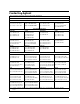
Table 1-1. Service Test Equipment Required Equipment Spectrum Analyzer Critical Speci cations Freq. Accuracy 67 Hz Use* Recommended Model HP 8563E A, T Frequency Counter HP 5343A P Measuring Receiver HP 8902A P Oscilloscope Bandwidth: 100 MHz Accuracy: 10% any T Digital Voltmeter Resolution: 10 mV any T Tool Kit No substitute HP part number 08753-60023 T Power Meter (HP-IB) No substitute HP 436A Opt.
Table 1-2. Service Test Equipment (2 of 2) Required Equipment Critical Speci cations Use* Recommended Model Adapter BNC to Alligator Clip HP P/N 8120-1292 A Adapter APC-3.5 (m) to type-N (f) HP P/N 1250-1750 A, P Adapter APC-3.5 (f) to type-N (f) HP P/N 1250-1745 A, P Adapter APC-3.
Table 1-2. Required Tools T-8, T-10 and T-15 TORX screwdrivers Flat-blade screwdrivers|small, medium, and large 5/16-inch open-end wrench (for SMA nuts) 3/16, 5/16, and 9/16-inch hex nut drivers 5/16-inch open-end torque wrench (set to 10 in-lb) 2.
Principles of Microwave Connector Care Proper connector care and connection techniques are critical for accurate, repeatable measurements. Refer to the calibration kit documentation for connector care information. Prior to making connections to the network analyzer, carefully review the information about inspecting, cleaning and gaging connectors. Having good connector care and connection techniques extends the life of these devices. In addition, you obtain the most accurate measurements.
Table 1-3.
Analyzer Options Available Option 003, 3 GHz Operation This option extends the maximum source and receiver frequency of the analyzer to 3 GHz. Option 004, Step Attenuator This option provides a source output power range from 085 to +10 dBm. Option 006, 6 GHz Operation This option extends the maximum source and receiver frequency of the analyzer to 6 GHz.
Option 1CP, Rack Mount Flange Kit With Handles This option is a rack mount kit containing a pair of anges and the necessary hardware to mount the instrument with handles attached in an equipment rack with 482.6 mm (19 inches) spacing. Option AFN, add 50 Test Port Cable This option provides a second type-N male to type-N male test port cable and a type-N female to type-N female adapter. Instructions are included for storing a new internal calibration to account for the e ects of this cable.
Service and Support Options Hewlett-Packards o ers many repair and calibration options for your analyzer. Contact the nearest Hewlett-Packard sales or service o ce for information on options available for your analyzer. See the table titled \Hewlett-Packard Sales and Service O ces" in Chapter 15.
System Veri cation and Performance Tests 2 How to Test the Performance of Your Analyzer To obtain the same quality of performance testing that Hewlett-Packard has administered at the factory, you must perform: the system veri cation procedure AND all of the performance test procedures. This quality of performance testing guarantees that the analyzer is performing within all of the published speci cations.
Sections in this Chapter HP 8752C System Veri cation HP 8752C Performance Tests 1. Re ection Test Port Output Frequency Range and Accuracy 2. Re ection Test Port Output Power Range and Level Linearity (HP 8752C without Option 004) 3. Re ection Test Port Output Power Range and Level Linearity (HP 8752C with Option 004) 4. Transmission Test Port Input Noise Floor Level (HP 8752C without Option 075) 5. Transmission Test Port Input Noise Floor Level (HP 8752C with Option 075) 6. Test Port Crosstalk 7.
HP 8752C System Veri cation Equipment For standard HP 8752C network analyzer: Calibration kit (50 , type-N) : : : : : : : : : : : : : : : : : : : : : : : : : : : : : : : : : : : : : : : : : : HP 85032B Cable type-N (50 ) 24-inch : : : : : : : : : : : : : : : : : : : : : : : : : : : : : : : : : : : : HP P/N 8120-4781 Printer : : : : : : : : : : : : : : : : : : : : : : : : : : : : : : : : : : : : : : : : : : HP ThinkJet, DeskJet, LaserJet For the HP 8752C with Option 075: Calibration kit (75 , type-N) : : : :
System Veri cation Cycle and Kit Recerti cation The recommended system veri cation cycle is every six months. HewlettPackard also suggests the calibration kit be recerti ed annually. For more information about the kit recerti cation, refer to the HP 85032B 50 Type-N Calibration Kit Operation and Service Manual or HP 85036B 75 Type-N Calibration Kit Operation and Service Manual. Measurement Uncertainty Associated with any analyzer are measurement errors that add uncertainty to the measured results.
Figure 2-1.
HP 8752C Type-N Test Port Characteristics (50 System) Directivity Frequency Range Speci cation Measurement Uncertainty 300 kHz to 1.3 GHz 40 dB1 1.3 GHz to 3.0 GHz 35 dB 3.0 GHz to 6.0 GHz 30 dB 63.30 dB 62.51 dB 63.30 dB Speci cation Measurement Uncertainty 300 kHz to 1.3 GHz 30 dB 1.3 GHz to 3.0 GHz 25 dB 3.0 GHz to 6.0 GHz 20 dB 62.51 dB 62.88 dB 62.88 dB Speci cation Measurement Uncertainty 300 kHz to 1.3 GHz 23 dB 1.3 GHz to 3.0 GHz 20 dB 3.0 GHz to 6.0 GHz 16 dB 62.
Load Match Frequency Range Speci cation Measurement Uncertainty 300 kHz to 1.3 GHz 23 dB1 1.3 GHz to 3.0 GHz 20 dB 3.0 GHz to 6.0 GHz 18 dB 60.40 dB 60.40 dB 60.92 dB 1 14 dB, 300 kHz to 10 MHz for analyzers with option 006 Transmission Tracking Frequency Range 300 kHz to 1.3 GHz 1.3 GHz to 3.0 GHz 3.0 GHz to 6.0 GHz Speci cation Measurement Uncertainty 60.2 dB 60.3 dB 60.5 dB 60.043 dB 60.086 dB 60.
Source Match (Transmission)* Frequency Range Speci cation Measurement Uncertainty 300 kHz to 1.3 GHz 23 dB 1.3 GHz to 3.0 GHz 20 dB 62.88 dB 63.30 dB *Option 004 may degrade transmission source match as much as 2 dB, resulting in up to 0.05 dB additional uncertainty in transmission tracking. Re ection Tracking Frequency Range Speci cation Measurement Uncertainty 60.2 dB 60.3 dB 60.2 dB 60.3 dB Speci cation Measurement Uncertainty 300 kHz to 1.3 GHz 23 dB 1.3 GHz to 3.0 GHz 20 dB 60.
System Veri cation Procedure 1. Switch the analyzer's line power ON. Press 4 5. 2. If you want a printout of the veri cation data, press 4 5 SYSTEM CONTROLLER 4 5 SERVICE MENU TEST OPTIONS RECORD ON . Otherwise, go to the next step.
7. Connect a type-N RF cable between the analyzer's re ection and transmission test ports. Press CONTINUE to test the system load match. NNNNNNNNNNNNNNNNNNNNNNNNNN 8. If you have activated the record feature, the system will automatically test its transmission tracking. Otherwise, press CONTINUE to access this test. NNNNNNNNNNNNNNNNNNNNNNNNNN 9. Press CONTINUE to end the system veri cation procedure. NNNNNNNNNNNNNNNNNNNNNNNNNN In case of di culty 1.
HP 8752C Performance Tests This portion of the manual contains performance tests which are part of the instrument calibration process. An instrument calibration includes the system veri cation, described in the previous section, and the performance tests. To test the complete set of instrument speci cations, both portions of the instrument calibration must be performed. Note Before performing these performance tests, check that the test equipment is operating to speci cation.
Equipment Required to Run the Performance Tests Description Quantity HP Model or Part Number Calibration kit, 50 type-N 1 HP 85032B Calibration kit, 75 type-N 1 HP 85036B Measuring Receiver 1 HP 8902A Frequency counter 1 HP 5343A Power meter 1 HP 436A, HP 437A, HP 438A Power sensor 1 HP 8482A Power sensor 1 HP 8481A Power sensor 1 HP 8483A Power sensor 1 HP 8483A Option H03 Printer 1 HP ThinkJet, DeskJet, LaserJet 110 dB step attenuator 1 HP 8496A 2-Way power splitter,
1. Re ection Test Port Output Frequency Range and Accuracy Speci cations Frequency Range 300 kHz to 1.
Procedure 1. Connect the equipment as shown in Figure 2-2. Press 4 5. PRESET Figure 2-2. Re ection Test Port Output Frequency Range and Accuracy Test Setup 2. Press 4 5 CW FREQ 4 5 4 5 4 5 4 5. Depending on the analyzer's options, record the frequency counter reading in the appropriate table (2 through 6) in the \Performance Test Record." 3. Repeat step 2 for each instrument's CW frequency listed in the appropriate table (2 through 6) in the \Performance Test Record.
2. Re ection Test Port Output Power Range and Level Linearity (For HP 8752C Analyzers without Option 004) Speci cations Power Range 020 to 015 dBm 015 to 0 dBm 0 to +5 dBm Power Level Linearity Relative to 05 dBm 60.5 dB 60.2 dB 60.
Procedure Power Range and Level Linearity for an HP 8752C or an HP 8752C Option 075 1. Connect the equipment as shown in Figure 2-3. Note For instruments with Option 075: a. use an HP 8483A (75 ) power sensor b. use tables 11 through 13 in the \Performance Test Record." For instruments with Option 075 and Option 003, use an HP 8483A Option H03 (75 ) power sensor. Figure 2-3. Re ection Test Port Output Power Range and Level Linearity Test Setup 2. Zero and calibrate the power meter.
pressing 4 panel. 5 dB REF on an HP 436A or 4 5 REL on an HP 438A power meter front 5. Press POWER 405 4 5 4 5 4 5. Record the power meter reading in the \Results Measured" column on the \Performance Test Record." 6. Utilizing the Power O set value listed in the \Performance Test Record," calculate the test port output power level linearity using the following formula: Power Level Linearity = Measured Value + Power O set 7. Record the result of your calculation on the \Performance Test Record." 8.
16. Utilizing the Power O set value listed in the \Performance Test Record (9 of 28)," calculate the Power Level Linearity using the following formula: Power Level Linearity = Measured Value + Power O set 17. Record the result of your calculation on the \Performance Test Record (9 of 28)." 18. Repeat steps 15, 16, and 17 for the other power levels listed in the \Performance Test Record (9 of 28)." Power Range and Level Linearity for an HP 8752C with Options 003 and 075 19.
3. Re ection Test Port Output Power Range and Level Linearity (HP 8752C with Option 004) Speci cations HP 8752C Option Power Range Option 004 085 to +10 dBm Options 004 and 075 085 to +8 dBm 1 Power Level Linearity1 60.2 dB (015 to +5 dBm) 60.5 dB (+5 to +10 dBm) 60.2 dB (015 to +5 dBm) 60.
and measured over its speci ed power range. The power level linearity is found by calculating the di erence between the power meter reading and the power o set listed in the \Performance Test Record." Procedure Power Range for an HP 8752C with Option 004 1. Connect the equipment as shown in Figure 2-4. Figure 2-4. Re ection Test Port Output Power Range Test Setup (HP 8752C Option 004) 2. Press 4 5 4CH 25 PRESET to set the analyzer up for transmission measurements. 3.
7. When the analyzer nishes the sweeps, record the data trace mean value (as shown on the upper right-hand corner of the analyzer display) on the \Performance Test Record (14 of 28)." 8. Press 4 5 POWER POWER RANGES RANGE 1 025 to 0 . Enter the power level value listed in the \Performance Test Record." For this power range, press 405 4 5 4 5 4 5. 9. Repeat steps 6, 7 and 8 for the other power ranges listed in the \Performance Test Record (14 of 28).
2. Zero and calibrate the power meter. For more information on how to perform this task, refer to the power meter's Operating and Service manual. 3. Press 4 5 4 5 CW FREQ 4 5 4 5 4 5 4 5. NNNNNNNNNNNNNNNNNNNNNNN PRESET MENU 3 0 0 k/m 4. Press POWER 405 4 5 4 5. Set the power meter cal factor for this CW frequency. On the power meter, set the current power level as the reference for relative power (dB) measurements by pressing 4 5 on an HP 436A or 4 5 on an HP 438A power meter's front panel. 5.
15. Press POWER 405 4 5 4 5 4 5. Record the power meter reading in the \Results Measured" column on the \Performance Test Record." 16. Utilizing the Power O set value listed in the \Performance Test Record," calculate the Power Level Linearity using the following formula: Power Level Linearity = Measured Value + Power O set 17. Record the result of your calculation on the \Performance Test Record." 18. Repeat steps 15, 16 and 17 for the other power levels listed in the \Performance Test Record.
4. Transmission Test Port Input Noise Floor Level (HP 8752C without Option 075) Speci cations Frequency Range IF Bandwidth 300 kHz to 1.3 GHz 3 kHz 300 kHz to 1.
Figure 2-6. Transmission Test Port Input Noise Floor Level Test Setup 1 2. Press 4 5 4MENU5 PRESET NNNNNNNNNNNNNNNNN POWER 405 4x15. If your analyzer has Option 003, press 4 If your analyzer has Option 006, press 4 5 435 4G/n5. STOP 5 465 4G/n5. STOP 3. Press 4 5 MEAS NNNNNNNNNNNNNNNNNNNNNNNNNNNNNNNNNNN NNNNN INPUT PORTS B 4DISPLAY5 DATA!MEMORY DATA/MEM . NNNNNNNNNNNNNNNNNNNNNNNNNNNNNNNNNNNNN NNNNNNNNNNNNNNNNNNNNNNNNNN 4. Connect the equipment as shown in Figure 2-7. Figure 2-7.
5. If your analyzer has Option 004, press 4 LIN MAG 4 5 AUTOSCALE . 5 MENU NNNNNNNNNNNNNNNNNNNNNNN NNNNNNNNNNNNNNNNNNNNNNNNNNNNN NNNNNNNNNNNNNNNNN POWER 0 4 5 485 455 4x15 4FORMAT5 SCALE REF If your analyzer does not have Option 004 installed, press 4 45 45 4 5 4 5 LIN MAG 4 5 AUTOSCALE . 5 MENU NNNNNNNNNNNNNNNNNNNNNNN 2 0 x1 FORMAT 6. Press 4 SINGLE .
Noise Floor Level at 3 GHz to 6 GHz (Option 006) with an IF BW of 10 Hz 13. Press 4 Figure 2-8. 5 435 4G/n5 4STOP5 465 4G/n5. START Connect the equipment as shown in Figure 2-8. Transmission Test Port Input Noise Floor Level Test Setup 1 14. Press 4 NNNNNNNNNNNNNNNNN 5 MENU POWER 405 4x15 4MENU5 NNNNNNNNNNNNNNNNNNNNNNNNNNNNNNNNNNNNNN NNNNNNNNNNNNNNNNNNNN TRIGGER MENU SINGLE . 15. When the sweep is nished, press 4 5 DATA!MEMORY Connect the equipment as shown in Figure 2-9.
16. If your analyzer has Option 004, press 4 TRIGGER MENU SINGLE . 5 MENU NNNNNNNNNNNNNNNNNNNNNNNNNNNNNNNNNNNNNN NNNNNNNNNNNNNNNNNNNN NNNNNNNNNNNNNNNNN POWER 0 4 5 485 455 4x15 4MENU5 If your analyzer does not have Option 004 installed, press 4 45 45 4 5 4 5 TRIGGER MENU SINGLE . 5 MENU NNNNNNNNNNNNNNNNNNNNNNNNNNNNNNNNNNNNNN NNNNNNNNNNNNNNNNNNNN 2 0 x1 NNNNNNNNNNNNNNNNN POWER 0 4 5 MENU 17. When the measurement is done, record the mean value. 18.
5. Transmission Test Port Input Noise Floor Level (HP 8752C with Option 075) Speci cations Frequency Range IF Bandwidth 300 kHz to 1.3 GHz 3 kHz 300 kHz to 1.
Figure 2-10. Transmission Test Port Input Noise Floor Level Test Setup 1 2. Press 4 5 4MENU5 PRESET NNNNNNNNNNNNNNNNN POWER 405 4x15 4MEAS5 3. To normalize the data trace, press 4 5 DISPLAY NNNNNNNNNNNNNNNNNNNNNNNNNNNNNNNNNNN NNNNN INPUT PORTS B . DATA!MEMORY DATA/MEM . NNNNNNNNNNNNNNNNNNNNNNNNNNNNNNNNNNNNN NNNNNNNNNNNNNNNNNNNNNNNNNN 4. Connect the equipment as shown in Figure 2-11. Figure 2-11. Transmission Test Port Input Noise Floor Level Test Setup 2 5.
7. Press 4 5 MARKER MODE MENU STATS ON NUMBER of GROUPS 4 5 4 5. NNNNNNNNNNNNNNNNNNNNNNNNNNNNNNNNNNNNNNNNNNNNNNNNNN NNNNNNNNNNNNNNNNNNNNNNNNNN MKR FCTN NNNNNNNNNNNNNNNNNNNNNNNNNNNNNNNNNNNNNNNNNNNNNNNNNN 5 4MENU5 NNNNNNNNNNNNNNNNNNNNNNNNNNNNNNNNNNNNNN TRIGGER MENU x1 8. When the trace is settled, record its mean value (as shown on the analyzer's display). 9.
6. Test Port Crosstalk Speci cations Frequency Range Test Port Impedance Test Port Crosstalk 50 100 dB 300 kHz to 3 GHz 50 100 dB 3 GHz to 6 GHz2 50 90 dB 300 kHz to 1.3 GHz 75 100 dB 1.3 GHz to 3 GHz 75 97 dB 300 kHz to 1.
Procedure 1. Connect the equipment as shown in Figure 2-12. Figure 2-12. Test Port Crosstalk Test Setup 2. Depending on the options that are currently installed in your analyzer, go to the appropriate following section to test the system crosstalk. Test Port Crosstalk for a Standard HP 8752C or an HP 8752C with Option 003 1. Press 4 press 4 5 NNNNNNNNNNNNNNNNNNNNNNNNNNNNNNNN TRANSMISSN . To set the test port power to 0 dBm, POWER 405 4x15. 5 4MEAS5 PRESET NNNNNNNNNNNNNNNNN MENU 2.
2. Press 4 5 45 45 4 AVERAGING ON . SCALE REF 2 5 5 4AVG5 x1 NNNNNNNNNNNNNNNNNNNNNNNNNNNNNNNNNNNNNN 3. Press 4 5 MKR FCTN 4. Press 4 5 NNNNNNNNNNNNNNNNN IF BW 415 405 4x15 AVERAGING FACTOR 455 4x15 NNNNNNNNNNNNNNNNNNNNNNNNNNNNNNNNNNNNNNNNN NNNNNNNNNNNNNNNNNNNNNNNNNNNNNNNNNNN NNNNNNNNNNNNNNNNNNNNNNNNNNNNNNNN MRK SEARCH ON TRACKING ON SEARCH:MAX .
2. Press 4 5 45 45 4 AVERAGING ON . SCALE REF 2 5 5 4AVG5 x1 NNNNNNNNNNNNNNNNNNNNNNNNNNNNNNNNNNNNNN 3. Press 4 5 MKR FCTN 4. Press 4 5 MENU NNNNNNNNNNNNNNNNN IF BW 415 405 4x15 NNNNNNNNNNNNNNNNNNNNNNNNNNNNNNNNNNNNNNNNNNNNNNNNNN AVERAGING FACTOR 455 4x15 NNNNNNNNNNNNNNNNNNNNNNNNNNNNNNNNNNNNNNNNN NNNNNNNNNNNNNNNNNNNNNNNNNNNNNNNNNNN NNNNNNNNNNNNNNNNNNNNNNNNNNNNNNNN MRK SEARCH ON TRACKING ON SEARCH:MAX .
7. System Trace Noise Speci cations Frequency Range Mode System Trace Noise (Magnitude)1 System Trace Noise (Phase)1 300 kHz to 1.3 GHz Transmission <0.006 dB rms <0.038 rms 300 kHz to 1.3 GHz Re ection <0.006 dB rms <0.038 rms 300 kHz to 3 GHz2 Transmission <0.006 dB rms <0.038 rms 300 kHz to 3 GHz2 Re ection <0.006 dB rms <0.038 rms 3 GHz to 6 GHz3 Transmission <0.010 dB rms <0.070 rms 3 GHz to 6 GHz3 Re ection <0.010 dB rms <0.
Procedure Re ection Trace Noise (Magnitude) 1. Connect the equipment as shown in Figure 2-13. Figure 2-13. Re ection Trace Noise Test Setup 2. Press 4 5 4 5 POWER 4 5 4 5 4 5 NUMBER of POINTS 4 5 4 5 4 5 4 5 4 5. 3. If you are testing a standard analyzer, press 4 5 CW FREQ 4 5 4 5 4 5 4 5.
6. Press 4 5 MENU NNNNNNNNNNNNNNNNNNNNNNNNNNNNNNNNNNNNNN NNNNNNNNNNNNNNNNNNNNNNNNNNNNNNNNNNNNNNNNNNNNNNNNNN TRIGGER MENU NUMBER of GROUPS 455 4x15. 7. When the measurement is done, record the s.dev (standard deviation) value shown in the upper right-hand corner of the analyzer display on the \Performance Test Record." Re ection Trace Noise (Phase) 8. Press 4 5 FORMAT 9. Press 4 5 MENU NNNNNNNNNNNNNNNNN PHASE 4SCALE 5 REF NNNNNNNNNNNNNNNNNNNNNNNNNNNNN AUTOSCALE .
Transmission Trace Noise (Phase) 15. Press 4 5 FORMAT 16. Press 4 5 MENU NNNNNNNNNNNNNNNNN PHASE 4SCALE 5 REF NNNNNNNNNNNNNNNNNNNNNNNNNNNNN AUTOSCALE . NNNNNNNNNNNNNNNNNNNNNNNNNNNNNNNNNNNNNN NNNNNNNNNNNNNNNNNNNNNNNNNNNNNNNNNNNNNNNNNNNNNNNNNN TRIGGER MENU NUMBER of GROUPS 455 4x15. 17. When the measurement is done, record the s. dev (standard deviation) value on the \Performance Test Record." In case of di culty 1. Replace the A10 digital IF board assembly. Rerun the test.
8.
Description This test veri es the magnitude dynamic accuracy of the analyzer's transmission test port. The test is performed at a CW frequency of 30 MHz. Procedure 1. On the HP 8902A, press the blue shift key and 4 5 4 5. Press the yellow shift key and 4 5. Press 4 5 to have the HP 8902A display linear readings (dBm). Press 4 5 4 5 4 5 4 5 4 5. 2. Set the HP 8496A to 20 dB. 3. On the analyzer, press 4 5 4 5 CW FREQ 4 5 4 5 4 5. Press NUMBER of POINTS 4 5 4 5 4 5. Press 4 5 IF BW 4 5 4 5 4 5.
Figure 2-15.
5. On the analyzer, press 4 5 TRANSMISSN 4 5 POWER 4 5 4 5. Using the analyzer's front panel knob, adjust the test port power for a reading of 030.000 dBm on the HP 8902A. Wait for the reading to stabilize. NNNNNNNNNNNNNNNNNNNNNNNNNNNNNNNN MEAS Note NNNNNNNNNNNNNNNNN MENU 0 x1 Ignore the UNCAL annunciation on the HP 8902A. 6. On the HP 8902A, press the blue shift key and 4 5. 7. On the analyzer, press 4 5 CALIBRATE MENU RESPONSE THRU . After the beep, press DONE: RESPONSE .
In case of di culty 1. If the test fails at all power levels, be sure you followed the recommended attenuator settings as listed in the \Performance Test Record." Repeat this performance test. 2. If the measured values are out of speci cations, the HP 8902A needs to be recalibrated. On the HP 8902A, press 4 5. Repeat this performance test. Be sure to press 4 5 when RECAL is shown on the measuring receiver display. 3. If this test fails at lower power levels: a.
9. Phase Dynamic Accuracy (HP 8752C - All Options) Speci cations Equipment There are no external equipment requirements to perform this test. Description This test veri es the phase dynamic accuracy of the analyzer's transmission port. The test is performed at a CW frequency of 30 MHz.
Procedure 1. Refer to the \Magnitude Dynamic Accuracy" section of the \Performance Test Record." For every Trans. Input Power, copy the result from the \Calculated Value" column and enter it in the \Magnitude Dynamic Accuracy Value" column of the Phase Dynamic Accuracy section of the \Performance Test Record." 2. For every Trans. Input Power, calculate \A" using the following formula: A = 10 3. Write the result in the \A" column of the \Performance Test Record." 4. For every Trans.
10. Compression Speci cations Frequency Range 300 kHz to 1.3 GHz 1.3 GHz to 3 GHz2 3 GHz to 6 GHz3 Magnitude1 0.45 dB 0.45 dB 0.82 dB Phase1 4.2 4.2 5.
Procedure 1. Connect the equipment as shown in Figure 2-16. Figure 2-16. Compression Test Setup 2. Press 4 5 4MEAS5 PRESET 3. Press 4 5 AVG 4. Press 4 NNNNNNNNNNNNNNNNN IF BW 5 MENU NNNNNNNNNNNNNNNNNNNNNNNNNNNNNNNN TRANSMISSN . 415 405 4x15. NNNNNNNNNNNNNNNNNNNNNNN CW FREQ 455 405 4M/ 5. 5. Press SWEEP TYPE MENU POWER SWEEP 4 5 4 5 4 5. 6. Press 4 5 TRIGGER MENU SINGLE .
13. Press 4 4SCALE 5 REF 14. Press 4 5 15. Press 4 5 NNNNNNNNNNNNNNNNNNNNNNNNNNNNNNNNNNNNNN NNNNNNNNNNNNNNNNNNNN TRIGGER MENU SINGLE . At the end of the sweep, press AUTOSCALE . 5 MENU NNNNNNNNNNNNNNNNNNNNNNNNNNNNN MKR MKR NNNNNNNNNNNNNNNNNNNNNNNNNNNNNNNNNNNNNNNNNNNN MARKER 1 REF=1 NNNNNNNNNNNNNNNNNNNNNNNNNN MARKER 2 4MKR 4MKR 5 FCTN 5 NNNNNNNNNNNNNNNNNNNNNNNNNNNNNNNN NNNNNNNNNNNNNNNNNNNNNNNNNNNNNNNNNNN MKR SEARCH SEARCH: MAX .
Performance Test Record HP 8752C Performance Test Record (1 of 28) Calibration Lab Address: Report Number Date Last Calibration Date Customer's Name Performed by Model HP 8752C Serial No.
HP 8752C Performance Test Record (2 of 28) Hewlett-Packard Company Model HP 8752C Report Number Serial Number Date 77 1. Re ection Test Port Output Frequency Range and Accuracy (Standard HP 8752C) CW Frequencies Min. Results Measured Max. Measurement (MHz) (MHz) (MHz) (MHz) Uncertainty (MHz) 0.3 0.299 997 5.0 4.999 950 16.0 15.999 840 31.0 30.999 690 60.999 999 60.999 390 121.0 120.998 790 180.0 179.998 200 310.0 309.995 900 700.0 699.930 000 1 300.0 1 299.987 000 0.300 003 5.000 050 16.000 160 31.
HP 8752C Performance Test Record (3 of 28) Hewlett-Packard Company Model HP 8752C Report Number Serial Number Date 1. Re ection Test Port Output Frequency Range and Accuracy (HP 8752C Option 003) CW Frequencies Min. Results Measured Max. Measurement (MHz) (MHz) (MHz) (MHz) Uncertainty (MHz) 77 0.3 0.299 997 5.0 4.999 950 16.0 15.999 840 31.0 30.999 690 60.999 999 60.999 390 121.0 120.998 790 180.0 179.998 200 310.0 309.995 900 700.0 699.930 000 1 300.0 1 299.987 000 2 000.0 1 999.980 000 3 000.0 2 999.
HP 8752C Performance Test Record (4 of 28) Hewlett-Packard Company Model HP 8752C Report Number Serial Number Date 1. Re ection Test Port Output Frequency Range and Accuracy (HP 8752C Option 006) CW Frequencies Min. Results Measured Max. Measurement (MHz) (MHz) (MHz) (MHz) Uncertainty (MHz) 77 0.3 0.299 997 5.0 4.999 950 16.0 15.999 840 31.0 30.999 690 60.999 999 60.999 390 121.0 120.998 790 180.0 179.998 200 310.0 309.995 900 700.0 699.930 000 1 300.0 1 299.987 000 2 000.0 1 999.980 000 3 000.0 2 999.
HP 8752C Performance Test Record (5 of 28) Hewlett-Packard Company Model HP 8752C Report Number Serial Number Date 1. Re ection Test Port Output Frequency Range and Accuracy (HP 8752C Option 075) CW Frequencies Min. Results Measured Max. Measurement (MHz) (MHz) (MHz) (MHz) Uncertainty (MHz) 77 0.3 0.299 997 5.0 4.999 950 16.0 15.999 840 31.0 30.999 690 60.999 999 60.999 390 121.0 120.998 790 180.0 179.998 200 310.0 309.995 900 700.0 699.930 000 1 300.0 1 299.
HP 8752C Performance Test Record (6 of 28) Hewlett-Packard Company Model HP 8752C Report Number Serial Number Date 1. Re ection Test Port Output Frequency Range and Accuracy (HP 8752C Options 003 and 075) CW Frequencies Min. Results Measured Max. Measurement (MHz) (MHz) (MHz) (MHz) Uncertainty (MHz) 77 0.3 0.299 997 5.0 4.999 950 16.0 15.999 840 31.0 30.999 690 60.999 999 60.999 390 121.0 120.998 790 180.0 179.998 200 310.0 309.995 900 700.0 699.930 000 1 300.0 1 299.987 000 2 000.0 1 999.
HP 8752C Performance Test Record (7 of 28) Hewlett-Packard Company Model HP 8752C Report Number Serial Number Date 2. Re ection Test Port Output Power Range and Level Linearity (HP 8752C without Option 004) Test Settings Results Power Power Speci cation Measurement (dBm) Measured O set Level (dB) Uncertainty (dB) (dB) (dB) Linearity (dB) CW Frequency = 300 kHz 77 0 20.0 0 18.0 0 16.0 0 14.0 0 12.0 0 10.0 0 8.0 0 6.0 0 4.0 0 2.0 0.0 +2.0 +4.0 +5.
HP 8752C Performance Test Record (8 of 28) Hewlett-Packard Company Model HP 8752C Report Number Serial Number Date 2. Re ection Test Port Output Power Range and Level Linearity (HP 8752C without Option 004) Test Settings Results Power Power Speci cation Measurement (dBm) Measured O set Level (dB) Uncertainty (dB) (dB) (dB) Linearity (dB) CW Frequency = 1.3 GHz 77 020.0 018.0 016.0 014.0 012.0 010.0 08.0 06.0 04.0 02.0 0.0 +2.0 +4.0 +5.0 +15 +13 +11 +9 +7 +5 +3 +1 01 03 05 07 09 010 60.5 60.5 60.5 60.
HP 8752C Performance Test Record (9 of 28) Hewlett-Packard Company Model HP 8752C Report Number Serial Number Date 2. Re ection Test Port Output Power Range and Level Linearity (HP 8752C with Option 003, without Option 004) Test Settings Results Power Power Speci cation Measurement (dBm) Measured O set Level (dB) Uncertainty (dB) (dB) (dB) Linearity (dB) CW Frequency = 3.0 GHz 77 020.0 018.0 016.0 014.0 012.0 010.0 08.0 06.0 04.0 02.0 0.0 +2.0 +4.0 +5.
HP 8752C Performance Test Record (10 of 28) Hewlett-Packard Company Model HP 8752C Report Number Serial Number Date 2. Re ection Test Port Output Power Range and Level Linearity (HP 8752C with Option 006, without Option 004) Test Settings Results Power Power Speci cation Measurement (dBm) Measured O set Level (dB) Uncertainty (dB) (dB) (dB) Linearity (dB) CW Frequency = 6.0 GHz 77 020.0 018.0 016.0 014.0 012.0 010.0 08.0 06.0 04.0 02.0 0.0 +2.0 +4.0 +5.
HP 8752C Performance Test Record (11 of 28) Hewlett-Packard Company Model HP 8752C Report Number Serial Number Date 2. Re ection Test Port Output Power Range and Level Linearity (HP 8752C with Option 075, without Option 004) Test Settings Results Power Power Speci cation Measurement (dBm) Measured O set Level (dB) Uncertainty (dB) (dB) (dB) Linearity (dB) CW Frequency = 300 kHz 77 020.0 018.0 016.0 014.0 012.0 010.0 08.0 06.0 04.0 02.0 0.0 +2.0 +4.0 +5.
HP 8752C Performance Test Record (12 of 28) Hewlett-Packard Company Model HP 8752C Report Number Serial Number Date 2. Re ection Test Port Output Power Range and Level Linearity (HP 8752C with Option 075, without Option 004) Test Settings Results Power Power Speci cation Measurement (dBm) Measured O set Level (dB) Uncertainty (dB) (dB) (dB) Linearity (dB) CW Frequency = 1.3 GHz 77 020.0 018.0 016.0 014.0 012.0 010.0 08.0 06.0 04.0 02.0 0.0 +2.0 +4.0 +5.
HP 8752C Performance Test Record (13 of 28) Hewlett-Packard Company Model HP 8752C Report Number Serial Number Date 2. Re ection Test Port Output Power Range and Level Linearity (HP 8752C with Options 003 and 075, without Option 004) Test Settings Results Power Power Speci cation Measurement (dBm) Measured O set Level (dB) Uncertainty (dB) (dB) (dB) Linearity (dB) CW Frequency = 2 GHz 77 020.0 018.0 016.0 014.0 012.0 010.0 08.0 06.0 04.0 02.0 0.0 +2.0 +4.0 +5.
HP 8752C Performance Test Record (14 of 28) Hewlett-Packard Company Model HP 8752C Report Number Serial Number Date 3. Re ection Test Port Output Power Range (HP 8752C with Option 004) Power Range Power Level Speci cation Mean Value Measurement (dBm) Value (dB) (dB) Uncertainty (dB) (dB) 77 015 to +10 025 to 0 035 to 010 045 to 020 055 to 030 065 to 040 075 to 050 085 to 060 010 020 030 040 050 060 070 080 0 61.0 0 61.5 0 61.7 0 61.9 0 62.2 0 62.5 0 62.8 0 63.1 60.100 60.060 60.050 60.050 60.055 60.
HP 8752C Performance Test Record (15 of 28) Hewlett-Packard Company Model HP 8752C Report Number Serial Number Date 3. Re ection Test Port Output Power Level Linearity (HP 8752C with Option 004) Test Settings Results Power Power Speci cation Measurement (dBm) Measured O set Level (dB) Uncertainty (dB) (dB) Linearity (dB) (dB) CW Frequency = 300 kHz 77 0 15.0 0 12.0 0 10.0 0 8.0 0 6.0 0 4.0 0 2.0 0.0 +2.0 +4.0 +5.0 +10.
HP 8752C Performance Test Record (16 of 28) Hewlett-Packard Company Model HP 8752C Report Number Serial Number Date 3. Re ection Test Port Output Power Level Linearity (HP 8752C with Option 004) Test Settings Results Power Power Speci cation Measurement (dBm) Measured O set Level (dB) Uncertainty (dB) (dB) Linearity (dB) (dB) CW Frequency = 1.3 GHz 77 0 15.0 0 12.0 0 10.0 0 8.0 0 6.0 0 4.0 0 2.0 0.0 +2.0 +4.0 +5.0 +10.0 +10 +7 +5 +3 +1 01 03 05 07 09 010 015 6 0.2 6 0.2 6 0.2 6 0.2 6 0.2 6 0.2 6 0.
HP 8752C Performance Test Record (17 of 28) Hewlett-Packard Company Model HP 8752C Report Number Serial Number Date 3. Re ection Test Port Output Power Level Linearity (HP 8752C with Option 004) Test Settings Results Power Power Speci cation Measurement (dBm) Measured O set Level (dB) Uncertainty (dB) (dB) Linearity (dB) (dB) CW Frequency = 3 GHz 77 0 15.0 0 12.0 0 10.0 0 8.0 0 6.0 0 4.0 0 2.0 0.0 +2.0 +4.0 +5.0 +10.
HP 8752C Performance Test Record (18 of 28) Hewlett-Packard Company Model HP 8752C Report Number Serial Number Date 3. Re ection Test Port Output Power Level Linearity (HP 8752C with Options 004 and 006) Test Settings Results Power Power Speci cation Measurement (dBm) Measured O set Level (dB) Uncertainty (dB) (dB) (dB) Linearity (dB) CW Frequency = 6 GHz 77 0 15.0 0 12.0 0 10.0 0 8.0 0 6.0 0 4.0 0 2.0 0.0 +2.0 +4.0 +5.0 +10.0 +10 +7 +5 +3 +1 01 03 05 07 09 010 015 6 0.2 6 0.2 6 0.2 6 0.2 6 0.2 6 0.
HP 8752C Performance Test Record (19 of 28) Hewlett-Packard Company Model HP 8752C Report Number Serial Number Date 3. Re ection Test Port Output Power Level Linearity (HP 8752C with Options 004 and 075) Test Settings Results Power Power Speci cation Measurement (dBm) Measured O set Level (dB) Uncertainty (dB) (dB) (dB) Linearity (dB) CW Frequency = 300 kHz 77 0 15.0 0 12.0 0 10.0 0 8.0 0 6.0 0 4.0 0 2.0 0.0 +2.0 +4.0 +5.0 +8.
HP 8752C Performance Test Record (20 of 28) Hewlett-Packard Company Model HP 8752C Report Number Serial Number Date 3. Re ection Test Port Output Power Level Linearity (HP 8752C with Options 004 and 075) Test Settings Results Power Power Speci cation Measurement (dBm) Measured O set Level (dB) Uncertainty (dB) (dB) (dB) Linearity (dB) CW Frequency = 1.3 GHz 77 0 15.0 0 12.0 0 10.0 0 8.0 0 6.0 0 4.0 0 2.0 0.0 +2.0 +4.0 +5.0 +8.0 +10 +7 +5 +3 +1 01 03 05 07 09 010 013 6 0.2 6 0.2 6 0.2 6 0.2 6 0.2 6 0.
HP 8752C Performance Test Record (21 of 28) Hewlett-Packard Company Model HP 8752C Report Number Serial Number Date 3. Re ection Test Port Output Power Level Linearity (HP 8752C with Options 003, 004, and 075) Test Settings Results Power Power Speci cation Measurement (dBm) Measured O set Level (dB) Uncertainty (dB) (dB) (dB) Linearity (dB) CW Frequency = 2 GHz 77 0 15.0 0 12.0 0 10.0 0 8.0 0 6.0 0 4.0 0 2.0 0.0 +2.0 +4.0 +5.0 +8.
HP 8752C Performance Test Record (22 of 28) Hewlett-Packard Company Model HP 8752C Report Number Serial Number Date 4. Transmission Test Port Input Noise Floor Level (HP 8752C without Option 075) Frequency Range IF BW Speci cation Calculated Measurement (dBm) Value Uncertainty (dB) HP 8752C Standard ONLY 77 300 kHz to 1.3 GHz 300 kHz to 1.
HP 8752C Performance Test Record (23 of 28) Hewlett-Packard Company Model HP 8752C Report Number Serial Number Date 77 5. Transmission Test Port Input Noise Floor Level (HP 8752C with Option 075) Frequency Range IF BW Spec. Calculated Measurement (dBm) Value Uncertainty (dB) 300 kHz to 1.3 GHz 300 kHz to 1.
HP 8752C Performance Test Record (24 of 28) Hewlett-Packard Company Model HP 8752C Report Number Serial Number Date 6. Test Port Crosstalk (HP 8752C All Options) Frequency Range Speci cation Measured Value (dBm) 77 Standard HP 8752C Measurement Uncertainty (dB) 300 kHz to 1.3 GHz 0100 dB N/A 300 kHz to 3.0 GHz 0100 dB N/A 300 kHz to 3.0 GHz 3.0 GHz to 6.0 GHz 0100 dB 0100 dB N/A N/A 300 kHz to 1.3 GHz 0100 dB N/A 300 kHz to 1.3 GHz 1.3 GHz to 3.
HP 8752C Performance Test Record (25 of 28) Hewlett-Packard Company Model HP 8752C Report Number Serial Number Date 7. System Trace Noise (HP 8752C All Options) Mode IF BW Speci cation Measured Measurement (dBm) Value Uncertainty (dB) (dB) 77 Standard HP 8752C Re ection Magnitude Re ection Phase Transmission Magnitude Transmission Phase 3 kHz 3 kHz 3 kHz 3 kHz <0.006 dB rms <0.038 rms <0.006 dB rms <0.
HP 8752C Performance Test Record (26 of 28) Hewlett-Packard Company Model HP 8752C Report Number Serial Number Date 8. Magnitude Dynamic Accuracy Trans. Port HP 8496A Trans. Port HP 8902A Measured Input Power Setting (dB) (dB) Value (dB) (dB) (dB) 77 020 030 040 050 060 070 080 090 0100 0110 10 20 30 40 50 60 70 80 90 100 Spec. (dB) Meas. Uncer. (dB) 0.058 0.050 0.050 0.053 0.060 0.115 0.285 0.860 2.500 5.400 60.02 60.02 60.04 60.06 60.08 60.14 60.16 60.18 60.20 60.
HP 8752C Performance Test Record (27 of 28)) Hewlett-Packard Company Model HP 8752C Report Number Serial Number Date 9. Phase Dynamic Accuracy Magnitude A B Calculated Spec. Meas. Dynamic Value (degrees) Uncert. Accuracy (degrees) Value 77 Trans. Port Input Power (dB) 020 030 040 050 060 070 080 090 0100 0110 2-76 System Veri cation and Performance Tests 0.46 0.35 0.36 0.38 0.40 0.70 1.90 6.00 18.00 55.
HP 8752C Performance Test Record (28 of 28) Hewlett-Packard Company Model HP 8752C Report Number Serial Number Date 10. Compression Spec. Meas. (dB) Uncert. 77 CW Freq.(GHz) 0.05 1.00 1.30 Magnitude Value (dB) 0.45 0.45 0.45 N/A N/A N/A Phase Value (degrees) Spec. Meas. (degrees) Uncer. (dB) 4.2 4.2 4.
3 Adjustments and Correction Constants The accuracy of the analyzer is achieved and maintained through mechanical adjustments and correction constants. The correction constants are empirically derived data that is stored in memory. Correction constants re ne the analyzer's measurements and de ne its operation.
If the analyzer displays one of these messages, check: the test setup the line power the HP-IB connections and addresses the model number After the problem has been identi ed and corrected, repeat the test. TROUBLE! CHECK SET-UP AND START OVER Check your setup against the illustrated test setup and repeat the test. Perform Adjustments in This Order When performing more than one adjustment, perform them in this order: 1. A9 CC Jumper Position Procedure 2. EEPROM Backup Disk Procedure 3.
Note If you have replaced the CPU board, or if the analyzer has lost all of its correction constants perform the adjustments in the order listed below (from top to bottom): 1. A9 CC Jumper Position Procedure 12. Serial Number Correction Constant (Test #55) 13. Option Number Correction Constant (Test #56) 16. Model Number Correction Constant 14. Initialize EEPROMs (Test #58) 16. Model Number Correction Constant 7. Display Intensity Adjustments (Test #49) 17. Vertical Position and Focus Adjustments 18.
Analyzer Cover Removal Typically, when performing the analyzer's adjustment procedures, only the top cover needs to be removed (to adjust the A9CC jumper position). To remove the top cover: 1. Remove the upper rear stando s. 2. Loosen the top cover retaining screw. 3. Slide back the cover.
1. A9 CC Jumper Position Procedure A9 CC (Correction Constant) Jumper Position To change the correction constants, you must move the A9 CC jumper to the ALT (alter) position. The analyzer is shipped (and should be operated) with the A9 CC jumper in the NRM (normal) position. Procedure Caution Switch o the analyzer's line power before removing or installing assemblies.
Figure 3-1.
1. Remove the analyzer top cover (see the section titled \Analyzer Cover Removal," located earlier in this chapter). 2. Remove the PC board stabilizer (item 1, Figure 3-1). 3. Remove the A9 CPU assembly by pulling on the white lifters. Figure 3-2. NRM (Normal) and ALT (Alter) Positions of A9 CC Jumper 4. Move the A9 CC jumper to the ALT position. Refer to Figure 3-2. 5. Reinstall the A9 assembly and run the correction constant routine(s). 6. Return the A9 CC jumper to the NRM position (see \1.
2. Source Default Correction Constants (Test #44) Equipment No equipment is required to perform this adjustment. Warm-up time 5 minutes Description and Procedure This internal adjustment test writes default correction constants for rudimentary source power accuracy. This adjustment must be performed before the \Source Pretune Correction Constants (Test #45)" procedure. 1. Put the A9 CC jumper in the ALT position (see \1. A9 CC Jumper Position Procedure"). 2. Press 4 5. 3.
3. Source Pretune Default Correction Constants (Test #45) Equipment No equipment is required to perform this adjustment. Warm-up time 30 minutes Description and Procedure This adjustment generates two default correction constants which pretune the YIG oscillators to insure proper phase lock. 1. Put the A9 CC jumper in the ALT position (see \1. A9 CC Jumper Position Procedure"). 2. Press 4 5. 3. Press 4 5 SERVICE MENU TESTS 4 5 4 5. 4. When the analyzer displays *Pretune Def press EXECUTE TEST . 5.
4. Analog Bus Correction Constants (Test #46) Equipment No equipment is required for this adjustment. Warm-up time 30 minutes Description and Procedure This procedure calibrates the analog bus using three reference voltages: ground, +0.37V and +2.5V. It then stores the calibration data as correction constants in EEPROM. 1. Put the A9 CC jumper in the ALT position (see \1. A9 CC Jumper Position Procedure"). 2. Press 4 5. 3. Press 4 5 SERVICE MENU TESTS 4 5 4 5.
5. RF Output Power Correction Constants (Test #47) Figure 3-3. Source Adjustment Setup Equipment Required Item For 50 Analyzers HP-IB cable (2) HP 10833A/B/C/D For 75 Analyzers HP 10833A/B/C/D Power meter HP 436A Option 022 or HP 438A HP 436A Option 022 or HP 438A Power sensor HP 8482A* HP 8483A Option HO3 *Use HP 8481A Option 006 above 4.2 GHz Warm-up time 30 minutes Description and Procedure Several correction constants improve the output power level accuracy of the internal source.
3. Press 4 5 SERVICE MENU TESTS 4 5 4 5 EXECUTE TEST YES to write default correction constants for rudimentary source power accuracy. 4. Press 4 5 4 5 INPUT PORTS R to measure input R. 5. Press 4 5 SYSTEM CONTROLLER SET ADDRESSES ADDRESS: P MTR/HPIB to see the address at which the analyzer expects to nd the power meter (the default address is 13). Refer to the power meter manual as required to observe or change its address to 13. 6.
NNNNNNNNNNNNNNNNNNNNNNNNNNNNNNNN CLEAR LIST : press the softkey to erase the entire table, NNNNNNNNNNNNNN DONE : press the softkey when a table is complete and correct. 8. Press the appropriate softkeys to build a sensor calibration table. Note The Sensor's reference calibration factor is the calibration factor for 50 MHz. 9. Carefully zero and calibrate the power meter/sensor (refer to the power meter/sensor manual as required). Source Correction Routine 10.
6. Source Pretune Correction Constants (Test #48) Equipment Required No equipment is required to perform this adjustment. Warm-up time 30 minutes Description and Procedure This adjustment generates two correction constants which pretune the YIG oscillators to insure proper phase lock. 1. Put the A9 CC jumper in the ALT position (see \1. A9 CC Jumper Position Procedure"). 2. Press 4 5. 3. Press 4 5 SERVICE MENU TESTS 4 5 4 5. 4. When the analyzer displays: Pretune Cor press EXECUTE TEST .
7. Display Intensity Adjustments (Test #49) Equipment Required Item Photometer Model Number Tektronix J16 Photometer probe Tektronix J6503 Light occluder Tektronix 016-0305-00 Warm-up time 30 minutes Description and Procedure There are three display intensity adjustments: 1. background 2. maximum 3. operating default Perform these adjustments when either the A19 GSP, A9 CPU, or A18 display assemblies are replaced (as indicated in \Assembly Replacement and Post-Repair Procedures").
3. Press 4 5 SERVICE MENU TESTS 4. The analyzer should display: Intensity Cor 0ND0 NNNNNNNNNNNNNNNNNNNNNNNNNNNNNNNNNNNNNN NNNNNNNNNNNNNNNNN SYSTEM Note 4495 4x15. The display could be so far out of adjustment that the annotation will be very di cult to read. NNNNNNNNNNNNNNNNNNNNNNNNNNNNNNNNNNNNNN NNNNNNNNNNN 5. Press EXECUTE TEST (top softkey) and YES (second from top softkey) at the prompt to alter the correction constants.
Figure 3-4. Maximum Intensity Adjustment Set-up 7. Press the top softkey. 8. Set the photometer probe to NORMAL. Press 4 5 on the photometer to switch it on and allow 30 minutes warm-up. Zero the photometer according to the manufacturer's instructions. The analyzer display should have an all white screen. 9. Center the photometer on the analyzer's display as shown in Figure 3-4. Adjust the analyzer's RPG knob to the maximum (clockwise) position.
Operating Default Intensity Adjustment This adjustment sets the display's default intensity level. The analyzer normally presets to the same intensity level that was last used. This level is stored in volatile memory. If the memory is lost, the analyzer will use the default display intensity to ensure that the display is visible and to eliminate concern that the display may not be functioning. 10. Press the top softkey on the analyzer to bring up the next display adjustment mode. 11.
8. IF Ampli er Correction Constants (Test #51) Equipment Required Item 50 Analyzers 75 Analyzers RF cable HP PN 8120-4781 HP PN 8120-4781 Pad attenuator N/A 50/75 min loss pad (2) N/A HP 8491A Option 020 HP 11852B Warm-up time 30 minutes Description and Procedure Figure 3-5. IF Ampli er Correction Constant Setup These correction constants compensate for possible discontinuities of signals greater than 030 dBm.
1. Put the A9 CC jumper in the ALT position (see \1. A9 CC Jumper Position Procedure"). 2. Press 4 5. 3. Press 4 5 SERVICE MENU TESTS 4 5 4 5. 4. Press EXECUTE TEST 5. When IF Step Cor PRESET NNNNNNNNNNNNNNNNNNNNNNNNNNNNNNNNNNNNNN NNNNNNNNNNNNNNNNN SYSTEM 51 x1 NNNNNNNNNNNNNNNNNNNNNNNNNNNNNNNNNNNNNN NNNNNNNNNNN 6. 7. 8. 9. appears on the display, press YES at the query to alter the correction constants. At the prompt, remove any cable or device from the re ection port. Press CONTINUE .
9. ADC O set Correction Constants (Test #52) Equipment No equipment is required to perform this adjustment. Warm-up time 30 minutes Description and Procedure These correction constants improve dynamic accuracy by shifting small signals to the most linear part of the ADC quantizing curve. 1. Put the A9 CC jumper in the ALT position (see \1. A9 CC Jumper Position Procedure"). 2. Press 4 5. 3. Press 4 5 SERVICE MENU TESTS 4 5 4 5.
10. Frequency Response Correction Constants (Tests #53 and #57) Equipment Required Item RF cable 50 Analyzers 75 Analyzers HP PN 8120-4781 HP PN 8120-2408 type-N calibration kit HP 85032B HP 85036B Warm-up time 30 minutes Description and Procedure Perform \5.
Note For open and short standards, you must select an additional softkey that indicates whether the test port is male or female. In this case, it is female (f). NNNNNNNNNNNNNN 7. Press DONE after the standard is measured. 8. Measure all three standard types (short, open, load). 9. Press DONE 1-PORT CAL to allow the analyzer to compute the calibration coe cients. This takes about 20 seconds. 10. Connect the RF cable between the re ection and transmission test ports. 11. Press THRU . 12.
11. Cavity Oscillator Frequency Correction Constants (Test #54) Equipment Required Item 50 Analyzers 75 Analyzers Low-pass lter HP PN 9135-0198 HP PN 9135-0198 RF cable HP PN 8120-4781 HP PN 8120-4781 50 to 75 minimum loss pad (2) N/A HP 11852B APC-3.5(f) to type-N(m) adapter 1250-1744 1250-1744 APC-3.5(m) to type-N(f) adapter 1250-1750 1250-1750 Warm-up time 30 minutes Description and Procedure Figure 3-6.
The nominal frequency of the cavity oscillator is 2.982 GHz, but it varies with temperature. This procedure determines the precise frequency of the cavity oscillator at a particular temperature by identifying a known spur. Note With the lter, the operator needs to distinguish between only two spurs, each of which should be 10 dB to 20 dB (3 to 4 divisions) above the trace noise. Without the lter, the target spur is one of four or ve spurs, each of which may be 0.002 to 0.
Note Each new span overlaps the previous span by 3 MHz (the center frequency increases by 2 MHz; the span is 5 MHz). Thus anything visible on the right half of the display on one set of sweeps will appear on the left half or center of the display. NNNNNNNNNNNNNN 7. Press NEXT repeatedly while watching the trace on each sweep and trying to spot the target spur. With the lter, the target spur will be one of two obvious spurs (see Figure 3-7).
Figure 3-7. Typical Target Spur Using Filter 10. Press SELECT and observe the display: DONE appears: the procedure has been performed successfully. Refer to \15. EEPROM Backup Disk Procedure" to store the new correction constants. If ND (not done) is displayed, repeat this procedure. Refer to \Source Troubleshooting" if ND is still displayed.
Spur Search Procedure without Filter Figure 3-8. Cavity Oscillator Frequency Correction Alternative Setup 11. Connect the test equipment as shown in Figure 3-8. 12. Without the lter, the target spur will appear in a variety of disguises. Often it will be di cult to identify positively; occasionally it will be nearly impossible to identify. Press CONTINUE as many times as necessary to thoroughly inspect the current span.
Figure 3-9. Typical Display of Four Spurs without Filter On occasion the target spur appears as one of a group of ve evenly spaced spurs, as in Figure 3-10. The target spur is again the fourth from the left (not the fth, right-most spur).
Figure 3-10. Typical Display of Five Spurs without Filter Figure 3-11 shows another variation of the basic four spur pattern: some up, some down and the target spur itself almost indistinguishable.
Figure 3-11. Variation of Display of Four Spurs without Filter 13. Rotate the RPG knob to position the marker on the target spur. Then press SELECT and observe the display: DONE appears: the procedure has been performed successfully. Refer to \15. EEPROM Backup Disk Procedure" to store the new correction constants. Return the A9 CC jumper to the NRM position (see \1. A9 CC Jumper Position Procedure"). If ND (not done) is displayed, repeat this procedure.
12. Serial Number Correction Constant (Test #55) Equipment No equipment is required for this adjustment. Warm-up time 5 minutes Description and Procedure This procedure customizes the replacement A9 CPU assembly by storing the analyzer's unique serial number as a correction constant in EEPROM. Caution Perform this procedure ONLY if the A9 CPU assembly has been replaced. 1. Put the A9 CC jumper in the ALT position (see \1. A9 CC Jumper Position Procedure"). 2.
6. If this procedure did not end with DONE: The serial number entered did not conform to the required format, or a valid serial number was already stored. In any case: Con rm that the serial number is correct, and repeat this procedure. Contact HP if the procedure still does not end with DONE. 7. To check the serial number recognized by the analyzer, press 4 5 4 5 SERVICE MENU FIRMWARE REVISION . The analyzer displays the new serial number (SER. NO.). If not, repeat steps 3 through 6. 8. Refer to \15.
13. Option Numbers Correction Constant (Test #56) Equipment No equipment is required for this adjustment. Warm-up time 5 minutes Figure 3-12.
Description and Procedure Special information is stored in the A9 CPU assembly if an analyzer has any of (or any combination of) these options: 003 (3 GHz operation) 004 (attenuator) 006 (6 GHz operation) 010 (time domain) This procedure restores that information after an A9 CPU assembly has been replaced. Perform this procedure only if: the analyzer has one or more of the above options, and the A9 CPU assembly has been replaced, and the serial number correction constant procedure has been performed. 1.
5. Press 4 5 SYSTEM NNNNNNNNNNNNNNNNNNNNNNNNNNNNNNNNNNNNNN NNNNNNNNNNNNNNNNN SERVICE MENU TESTS 4565 4x15. When the display shows: Option Cor NNNNNNNNNNNNNNNNNNNNNNNNNNNNNNNNNNNNNN NNNNNNNNNNN press EXECUTE TEST . Press YES at the query to alter the correction constant and observe the analyzer's display: If DONE is displayed: the adjustment is complete. Continue with step 6.
14. Initialize EEPROMs (Test #58) This service internal test performs the following functions: destroys all correction constants and all un-protected options initializes certain EEPROM address locations to zeros replaces the display intensity correction constants with default values Note This routine will not alter the serial number or Options 003, 006 and 010 correction constants. 1.
15. EEPROM Backup Disk Procedure Equipment Required Item HP Model CS80 disk drive HP 9122 HP-IB cable HP 10833A/B/C/D 3.5-inch disk blank disk or supplied EEPROM Calibration Data Disk Warm-up time None Description and Procedure Figure 3-13. EEPROM Backup Procedure Setup A unique EEPROM Calibration Data Disk is shipped from the factory with each analyzer. This disk is a record of the calibration constants (CCs) stored in EEPROM on the A9 CPU assembly.
Retrieve correction constant data from the EEPROM Calibration Data Disk if you need to replace the A9 CPU board assembly. How to Make an EEPROM Backup Disk and Store CCs and Data to It 1. Set the disk drive to HP-IB address 00. Insert a disk in drive 0. 2. Connect the instruments as shown in Figure 3-13. Switch on the analyzer rst, followed by the disk drive. 3. Press 4 5 SYSTEM CONTROLLER . 4. Press 4 5 SELECT DISK CONFIGURE EXT DISK . Set the disk address, disk unit number, and volume number to 0. 5.
How to Recall CC Data from the EEPROM Disk into the Analyzer 1. Set the disk drive to HP-IB address 00 and insert the EEPROM Disk. 2. Connect the instruments as shown in Figure 3-13. 3. Put the A9 CC jumper in the ALT position (see \1. A9 CC Jumper Position Procedure"). 4. Install the new A9 assembly. 5. Switch on the disk drive and then the analyzer: If the display is dark: Press 4 5 MORE (bottom softkey) ADJUST DISPLAY (fourth softkey from top) INTENSITY (top softkey) and then turn the RPG knob.
13. Return the A9 CC jumper to the NRM position (see \1. A9 CC Jumper Position Procedure"). In case of di culty, refer to the chapter titled \Start Troubleshooting Here.
16. Model Number Correction Constant (Option 075 Only) Equipment No equipment is required for this adjustment. Warmup time 5 minutes Description and Procedure This procedure sets an EEPROM bit for HP 8752C analyzers with Option 075 so that certain system default values will be correct after the A9 CPU assembly rmware is replaced. Firmware and A9 CPU assemblies are shipped with the bit set correctly for HP 8752C analyzers without Option 075.
17. Vertical Position and Focus Adjustments Equipment Narrow, non-conductive, athead screwdriver, 2-inches long Warmup time 30 minutes Description and Procedure Only vertical position and focus, can be adjusted in the eld (this includes both customers and service centers). These adjustments are optional and should rarely be required. Caution Any other adjustments to the display will void the warranty. Vertical Position Adjustment 1.
Figure 3-14. Vertical Position and Focus Adjustment Controls 2. Insert a narrow, non-conductive, at head screw driver (at least 2-inches long) into the vertical position hole. See Figure 3-14. 3. Adjust the control until the softkey labels are aligned with the softkeys. Focus Adjustment 4. Use the same screwdriver to adjust the focus until the display is the most readable.
18. Display Degaussing (Demagnetizing) Equipment Any CRT demagnetizer or bulk tape eraser Warm-up time 5 minutes Description and Procedure All color monitors are susceptible to external magnetic elds. The usual symptom is a discoloration or slight dimming, usually occurring near the top left corner of the analyzer's display. In extreme cases, a total color shift may be observed; for example, a trace that was red may shift to green.
19. Fractional-N Frequency Range Adjustment Equipment Required No equipment is required to perform this adjustment procedure. Warm-up time 30 minutes Description and Procedure This adjustment centers the fractional-N VCO (voltage controlled oscillator) in its tuning range to insure reliable operation of the analyzer. 1. Remove the analyzer right side panel. 2. Press 4 5. 3. Press 4 5 DUAL CHAN ON 4 5 NUMBER of POINTS 4 5 4 5 COUPLED CH OFF . 4.
Figure 3-15. FN VCO TUNE Adjustment Location 7. Observe the analyzer display for the results of the adjustment. a. Refer to Figure 3-15. If the marker value is less than 7, the adjustment procedure is complete.
Figure 3-16. Fractional-N Frequency Range Adjustment Display b. If the marker value is greater than 7, readjust FN VCO ADJ to 7 (refer to Figure 3-14). Perform steps 2 through 7 to con rm that the channel 1 and channel 2 markers respectively are still above and below the reference line. c. If the adjustment cannot be performed correctly, replace the A14 board assembly.
20. Frequency Accuracy Adjustment Equipment Required Item HP Model Number 50 to 75 minimum loss pad* HP 11852B type-N cable HP PN 8120-4781 type-N(f) to BNC(m) adapter HP PN 1250-0077 Frequency counter HP 5343A * Option 075 analyzers only. Warm-up time 30 minutes Figure 3-17. Re ection Test Port Output Frequency Accuracy Adjustment Setup Note For 75 analyzers, insert an HP 11852B 50 to 75 minimum loss pad and adapters between frequency counter port and type-N cable.
Description and Procedure This adjustment sets the VCXO (voltage controlled crystal oscillator) frequency to maintain the analyzer's frequency accuracy. 1. Remove the analyzer's top cover and connect the equipment as shown in Figure 3-17. 2. Press 4 5. 3. Press 4 5 CW FREQ 4 5 4 5 and note the frequency: Frequency = 50 MHz 6500 Hz: no adjustment is required.
21. High/Low Band Transition Adjustment Equipment Required No equipment is required for this adjustment procedure. Warm-up time 30 minutes Description and Procedure This adjustment centers the VCO (voltage controlled oscillator) of the A12 reference assembly for reliable high band and low band operation. 1. Remove the top cover (see \1. A9CC Jumper Position Procedure"). Remove the PC board stabilizer and place the A12 assembly on an extender board. Use extension SMB cables as needed. 2. Press 4 5. 3.
Figure 3-19. High/Low Band Transition Adjustment Trace To adjust: turn VCO TUNE (see Figure 3-20) to position the left half of the trace to 06125 mV. Then adjust HBLB to position the right half of the trace 125 to 175 mV (about 1 1/2 divisions) higher than the left half. Figure 3-20.
7. In some cases, the VCO TUNE adjustment may need to be performed rst. If you are having trouble with the high low band adjustment, perform the following procedure: a. Press: 4 5 SERVICE MENU ANALOG BUS ON NNNNNNNNNNNNNNNNNNNNNNNNNNNNNNNNNNNNNN NNNNNNNNNNNNNNNNNNNNNNNNNNNNNNNNNNNNNNNNN SYSTEM 4START5 4105 4M/ 5 4STOP5 4105 4M/ 5 b. Press: 4MEAS5 NNNNNNNNNNNNNNNNNNNNNNNNNNNNNNNNNNNNNNNNNNNNNNNNNNNNNNNNNNN ANALOG IN Aux INPUT 4DISPLAY5 c.
22. Fractional-N Spur Avoidance and FM Sideband Adjustment Equipment Required Item HP Model Number Spectrum Analyzer HP 8563E RF Cable 50 , type-N, 24-inch HP P/N 8120-4781 Cable, 50 Coax, BNC (m) to BNC (m) HP 10503A Non-metallic Adjustment Tool HP P/N 8830-0024 Antistatic Wrist Strap HP P/N 9300-1367 Antistatic Wrist Strap Cord HP P/N 9300-0980 Static-control Table Mat and Earth Ground Wire HP P/N 9300-0797 50 to 75 Minimum Loss Pad* HP 11852B * Option 075 analyzers only.
Figure 3-21. Fractional-N Spur Avoidance and FM Sideband Adjustment Setup 3. Set the spectrum analyzer measurement parameters as follows: Reference Level : : : : : : : : : : : : : : : : : : : : : : : : : : : : : : : : : : : : : : : : : : : : : : : : : : : : : : : 0 dBm Resolution Bandwidth : : : : : : : : : : : : : : : : : : : : : : : : : : : : : : : : : : : : : : : : : : : : : : : : 100 Hz Center Frequency : : : : : : : : : : : : : : : : : : : : : : : : : : : : : : : : : : : : : : : : : : : 676.
4. On the HP 8752C, press 4 5 4 5 4 5 4 5. 5. Refer to Figure 3-22. Adjust the 100 kHz (R77) for a null (minimum amplitude) on the spectrum analyzer. The minimum signal may, or may not, drop down into the noise oor. PRESET CENTER 676.045105 M/ Figure 3-22. Location of API and 100 kHz Adjustments 6. On the spectrum analyzer, set the center frequency for 676.048105 MHz. 7. On the HP 8752C, press 4 5 4 5 4 5. 8. Adjust the API1 (R35) for a null (minimum amplitude) on the spectrum analyzer. 9.
16. On the HP 8752C, press 4 5 4 5 4 5. 17. Adjust the API4 (R47) for a null (minimum amplitude) on the spectrum analyzer. CENTER 676.000045 M/ In Case of Di culty 18. If this adjustment cannot be performed satisfactorily, repeat the entire procedure. If the adjustment is still unattainable, replace the A13 board assembly.
23. Source Spur Avoidance Tracking Adjustment Equipment Required Item HP Part Number BNC-alligator clip adapter 8120-1292 BNC cable 8120-1840 Warm-up time 30 minutes Description and Procedure This adjustment optimizes tracking between the YO (YIG oscillator) and the cavity oscillator when they are frequency o set to avoid spurs. Optimizing YO-cavity oscillator tracking minimizes uctuations in the phase-locked loop. 1.
2. Press 4 5. 3. Press 4 5 4 5 4 5 4 5 4 5 4 5 to generate a sweep from 375 MHz to 425 MHz. 4. Press 4 5 SERVICE MENU ANALOG BUS ON 4 5 ANALOG IN Aux Input 4 5 4 5 4 5 4 5 4 5 4 5 MARKER->REFERENCE to observe the phase-locked loop error voltage: If spikes are not visible on the display (see Figure 3-24): no adjustment is necessary. If spikes are excessive (see Figure 3-24): adjust the CAV ADJ potentiometer (see Figure 3-23) on the A3 source bias assembly to eliminate the spikes. 5.
4 Start Troubleshooting Here The information in this chapter helps you: Identify the portion of the analyzer that is at fault. Locate the speci c troubleshooting procedures to identify the assembly or peripheral at fault. To identify the portion of the analyzer at fault, follow these procedures: Step 1. Initial Observations Step 2. Con dence Test Step 3. HP-IB System Check Step 4.
Assembly Replacement Sequence The following steps show the sequence to replace an assembly in an HP 8752C Network Analyzer. 1. Identify the faulty group. Refer to the \Start Troubleshooting Here" chapter. Follow up with the appropriate troubleshooting chapter that identi es the faulty assembly. 2. Order a replacement assembly. Refer to the \Replaceable Parts" chapter. 3. Replace the faulty assembly and determine what adjustments are necessary.
Step 1. Initial Observations Initiate the Analyzer Self-Test 1. Disconnect all devices and peripherals from the analyzer. 2. Switch on the analyzer and press 4 5. 3. Watch for the indications in the order shown in Figure 4-1 to determine if the analyzer is operating correctly. PRESET Figure 4-1. LED Power-up Sequence If the Self-Test Failed 1. 2. 3. 4. Check the AC line power to the analyzer. Check the fuse (rating listed on rear panel, spare inside holder).
Step 2. Con dence Test The con dence test veri es that the circuits in the analyzer are functioning properly. However, it does not verify the accessories or the analyzer speci cations. The resulting measurement must fall within a limit testing window to pass the test. The window size is based on both source and receiver speci cations. The characteristics tested are combinations of: source match, re ection tracking, directivity, transmission tracking, noise oor, and crosstalk.
6. Press CONTINUE to run the \transmission crosstalk, noise oor" test. (With the record function on, this test will automatically run). There should be a PASS/FAIL result displayed on the analyzer. 7. Press CONTINUE and then connect the RF cable supplied with the analyzer between the re ection and transmission test ports. 8. Press CONTINUE to run the \transmission tracking, source/load match" test. There should be a PASS/FAIL result displayed on the analyzer. 9.
2. Press EXECUTE TEST . The analyzer now displays a brief description of the test and the test limits. 3. Press CONTINUE to begin the test. Connect an RF cable between the re ection and the transmission test ports, as prompted on the analyzer. 4. Press CONTINUE and notice the PASS/FAIL result.
Step 3. HP-IB Systems Check Check the analyzer's HP-IB functions with a known working passive peripheral (such as a plotter, printer, or disk drive). 1. Connect the peripheral to the analyzer using a good HP-IB cable.. 2. Press 4 5 SYSTEM CONTROLLER to enable the analyzer to control the peripheral. 3. Then press SET ADDRESSES and the appropriate softkeys to verify that the device addresses will be recognized by the analyzer.
If Using a Plotter or Printer 1. Ensure that the plotter or printer is set up correctly: power is on pens and paper loaded pinch wheels are down some plotters need to have P1 and P2 positions set 2. Press 4 5 and then PLOT or PRINT MONOCHROME . NNNNNNNNNNNNNN NNNNNNNNNNNNNNNNNNNNNNNNNNNNNNNNNNNNNNNNNNNNNNNNNN COPY If the result is a copy of the analyzer display, the printing/plotting features are functional in the analyzer.
4. Press 4 5 415 4M/ 5 4SAVE/RECALL5 START 4SAVE/RECALL5 NNNNNNNNNNNNNNNNNNNNNNNNNNNNNNNNNNNNNN NNNNNNNNNNNNNNNNNNNNNNNNNNNNNNNN SAVE STATE . Then press 4PRESET5 RECALL STATE . If the resultant trace starts at 1 MHz, HP-IB is functional in the analyzer. Continue with \Troubleshooting Systems with Multiple Peripherals," \Troubleshooting Systems with Controllers," or the \Step 4. Faulty Group Isolation" section in this chapter.
Step 4. Faulty Group Isolation Use the following procedures only if you have read the previous sections in this chapter and you think the problem is in the analyzer. These are simple procedures to verify the four functional groups in sequence, and determine which group is faulty. The four functional groups are: power supplies digital control source receiver Descriptions of these groups are provided in the \Theory of Operation" chapter.
Power Supply Check Check the Rear Panel LEDs Switch on the analyzer. Notice the condition of the two LEDs on the A15 preregulator at rear of the analyzer (see Figure 4-3). The upper (red) LED should be o . The lower (green) LED should be on. Figure 4-3. A15 Preregulator LEDs Check the A8 Post Regulator LEDs Remove the analyzer's top cover. Inspect the green LEDs along the top edge of the A8 post regulator assembly. All green LEDs should be on. The fan should be audible.
Digital Control Check Observe the Power Up Sequence Switch the analyzer power o , then on. The following should take place within a few seconds: On the front panel observe the following: 1. All six amber LEDs illuminate. 2. The amber LEDs go o after a few seconds, except the CH 1 LED. (See Figure 4-4). The display should come up bright and focused. Figure 4-4.
Verify Internal Tests Passed 1. Press 4 5 4 5 SERVICE MENU TESTS INTERNAL TESTS EXECUTE TEST . The display should indicate: NNNNNNNNNNNNNNNNNNNNNNNNNNNNNNNNNNNNNN NNNNNNNNNNNNNNNNN NNNNNNNNNNNNNNNNNNNNNNNNNNNNNNNNNNNNNNNNNNNN PRESET SYSTEM NNNNNNNNNNNNNNNNNNNNNNNNNNNNNNNNNNNNNN TEST 0 ALL INT PASS If your display shows the above message, go to step 2. Otherwise, continue with this step. If phase lock error messages are present, this test may stop without passing or failing.
2. Connect the equipment as shown in Figure 4-5. Item 50 Ohm NAs Power meter 75 Ohm NAs HP 436A, 437B, or 438A Power sensor HP 8482A HP 8483A Option H03* * special option power sensor Figure 4-5. Equipment Setup for Source Power Check 3. Switch on the instruments. Zero and calibrate the power meter. 4. On the analyzer, press 4 5 Stimulus 4 5 POWER 40 5 4 5 4 5 CW FREQ 4 5 4 5. The power meter should read approximately 020 dBm (085 dBm for Option 004). 5.
Receiver Check 1. Connect an RF cable directly between the re ection and transmission ports. 2. On the analyzer, press 4 5 4 5 TRANSMISSION 4 5 4 5 4 5. NNNNNNNNNNNNNNNNNNNNNNNNNNNNNNNNNNNNNN PRESET MEAS SCALE REF .5 x1 3. Notice the condition of the trace: it should resemble Figure 4-6 If the trace shows unexpected results, refer to the \Receiver Troubleshooting" chapter. Figure 4-6.
4-16 Start Troubleshooting Here
Figure 4-7.
Figure 4-7.
Figure 4-7.
5 Power Supply Troubleshooting Use this procedure only if you have read the \Start Troubleshooting Here" chapter. Follow the procedures in the order given, unless: an error message appears on the display, refer to \Error Messages" near the end of this chapter. the fan is not working, refer to \Fan Troubleshooting" in this chapter.
Assembly Replacement Sequence The following steps show the sequence to replace an assembly in an HP 8752C Network Analyzer. 1. Identify the faulty group. Refer to the \Start Troubleshooting Here" chapter. Follow up with the appropriate troubleshooting chapter that identi es the faulty assembly. 2. Order a replacement assembly. Refer to the \Replaceable Parts" chapter. 3. Replace the faulty assembly and determine what adjustments are necessary.
Simpli ed Block Diagram Figure 5-1 shows the power supply group in simpli ed block diagram form. Refer to the detailed block diagram of the power supply (Figure 5-8) located at the end of this chapter to see voltage lines and speci c connector pin numbers. Figure 5-1.
Start Here Check the Green LED and Red LED on A15 Switch on the analyzer and look at the rear panel of the analyzer. Check the two power supply diagnostic LEDs on the A15 preregulator casting by looking through the holes located to the left of the line voltage selector switch (see Figure 5-2). During normal operation, the bottom (green) LED is on and the top (red) LED is o . If these LEDs are normal, then A15 is 95% veri ed. Continue with \Check the Green LEDs on A8".
Check the Green LEDs on A8 1. Remove the top cover of the analyzer and locate the A8 post regulator. Use the location diagram under the top cover if necessary. 2. Check to see if the green LEDs on the top edge of A8 are all on. There are nine green LEDs (one is not visible without removing the PC board stabilizer). If all of the green LEDs on the top edge of A8 are on, there is a 95% con dence level that the power supply is veri ed.
Table 5-1. A8 Post Regulator Test Point Voltages TP Supply Range 1 +65V +64.6 to +65.4 2 AGND n/a 3 +5 VD +4.9 to +5.3 4 SDIS n/a 5 015V 6 012.6 VPP (probe power) 014.4 to 015.6 012.1 to 012.8 7 +15V +14.5 to +15.5 8 +5 VU +5.05 to +5.35 9 05.2 V 05.0 to 05.4 10 +22V +21.3 to +22.7 11 +6V +5.8 to +6.
If the Green LED on A15 is not On Steadily If the green LED is not on steadily, the line voltage is missing or is not enough to power the analyzer. Check the Line Voltage, Selector Switch, and Fuse 1. Check the main power line cord, line fuse, line selector switch setting, and actual line voltage to see that they are all correct. Figure 5-4 shows how to remove the line fuse, using a small at-bladed screwdriver to pry out the fuse holder. Figure 5-2 shows the location of the line voltage selector switch.
If the Red LED On A15 is On If the red LED is on or ashing, the power supply is shutting down. Use the following procedures to determine which assembly is causing the problem. Check the A8 Post Regulator 1. Switch o the analyzer. 2. Disconnect the cable A15W1 from the A8 post regulator (see Figure 5-5). 3. Switch on the analyzer and observe the red LED on A15. If the red LED goes out, the problem is probably the A8 post regulator.
Figure 5-5. Power Supply Cable Locations Verify the A15 Preregulator Verify that the A15 preregulator is supplying the correct voltages to the A8 post regulator. Use a voltmeter with a small probe to measure the output voltages of A15W1's plug. Refer to Table 5-2 and Figure 5-6. If the voltages are not within tolerance, replace A15. If the voltages are within tolerance, A15 is veri ed. Continue with \Check for a Faulty Assembly.
Table 5-2. Output Voltages Pin A15W1P1 (Disconnected) Voltages A8J2 (Connected) Voltages A15 Preregulator Mnemonic 1,2 +125 to +100 +68 to +72 +70V 3,4 +22.4 to +33.6 +17.0 to +18.4 +18V 5,6 022.4 to 033.6 017.0 to 018.4 018V 7 N/C N/C N/C 8 +9.4 to +14 +7.4 to +8.0 +8 V 9,10 09.4 to 014 06.7 to 07.3 08 V 11 +32 to +48 +24.6 to +26.6 +25V 12 N/C N/C N/C NOTE: The +5VD supply must be loaded by one or more assemblies at all times, or the other voltages will not be correct.
Figure 5-6.
Do the following: 1. Switch o the analyzer. 2. Ensure that A15W1 is reconnected to A8 (refer to Figure 5-5). 3. Remove or disconnect the assemblies listed in Table 5-3 one at a time and in the order shown. The assemblies are sorted from most to least accessible. Table 5-3 also lists any associated assemblies that receive power from the assembly that is being removed. After each assembly is removed or disconnected, switch on the analyzer and observe the red LED on A15.
Check the Operating Temperature The temperature sensing circuitry inside the A15 preregulator may be shutting down the supply. Make sure the temperature of the open air operating environment does not exceed 55 C (131 F), and that the analyzer fan is operating. If the fan does not seem to be operating correctly, refer to \Fan Troubleshooting" at the end of this procedure. If there does not appear to be a temperature problem, it is likely that A15 is faulty.
If the Green LEDs On A8 are not All On The green LEDs along the top edge of the A8 post regulator are normally on. Flashing LEDs on A8 indicate that the shutdown circuitry on the A8 post regulator is protecting power supplies from overcurrent conditions by repeatedly shutting them down. This may be caused by supply loading on A8 or on any other assembly in the analyzer. Remove A8, Maintain A15W1 Cable Connection 1. Switch o the analyzer. 2.
If the green LEDs are now on, the A15 preregulator and A8 post regulator are working properly and the trouble is excessive loading somewhere after the motherboard connections at A8. Continue with \Remove the Assemblies." Remove the Assemblies 1. Switch o the analyzer. 2. Install A8. Remove the jumper from A8TP2 (AGND) to chassis ground. 3. Remove or disconnect all the assemblies listed below (see Figure 5-5). Always switch o the analyzer before removing or disconnecting an assembly.
11. Switch o the analyzer. 12. Reinstall each assembly one at a time. Switch on the analyzer after each assembly is installed. The assembly that causes the green LEDs to go o or ash could be faulty. Note It is possible, however, that this condition is caused by the A8 post regulator not supplying enough current. To check this, reinstall the assemblies in a di erent order to change the loading. If the same assembly appears to be faulty, replace that assembly.
c. Make a list of these assemblies. d. Delete the following assemblies from your list as they have already been veri ed earlier in this section. A9 CPU A10 digital IF A11 phase lock A12 reference A13 fractional-N analog A14 fractional-N digital A18 display A19 graphics processor 5. Switch o the analyzer. 6. Of those assemblies that are left on the list, remove or disconnect them from the analyzer one at a time. Table 5-4 shows the best order in which to remove them.
Table 5-4. Recommended Order for Removal/Disconnection Assembly To Remove Removal or Disconnection Method Other Assemblies that Receive Power from the Removed Assembly 1. A3 Source 2. A7 Pulse Generator 3. A4 R Sampler 4. A5 A Sampler 5. A6 B Sampler 6. A2 Front Panel Interface Remove from Card Cage None Disconnect W17 A1 Front Panel Keyboard 7.
Error Messages Three error messages are associated with the power supplies functional group. They are shown here. POWER SUPPLY SHUT DOWN! One or more supplies on the A8 post regulator assembly is shut down due to one of the following conditions: overcurrent, overvoltage, or undervoltage. Refer to \If the Red LED On A15 is On" earlier in this procedure. POWER SUPPLY HOT! The temperature sensors on the A8 post regulator assembly detect an overtemperature condition.
Figure 5-7. Front Panel Probe Power Connector Voltages If the correct voltages are present, troubleshoot the probe. If the voltages are not present, check the +15V and 012.6V green LEDs on A8. If the LEDs are on, there is an open between the A8 assembly and the front panel probe power connectors. Put A8 onto an extender board and measure the voltages at the following pins: A8P2 pins 6 and 36 A8P2 pins 4 and 34 012.6 volts +15 volts If the LEDs are o , continue with \Check the Fuses and Isolate A8.
Check the Fuses and Isolate A8 1. Check the fuses associated with each of these supplies near the A8 test points. If these fuses keep burning out, a short exists. 2. Try isolating A8 by removing it from the motherboard connector, but keeping the cable A15W1 connected to A8J2. 3. Connect a jumper wire from A8TP2 to chassis ground. If either the +15V or 012.6V fuse blows, or the associated green LEDs do not light, replace A8. If the +15V and 012.
Fan Troubleshooting Fan Speeds The fan speed varies depending upon temperature. It is normal for the fan to be at high speed when the analyzer is just switched on, and then change to low speed when the analyzer is cooled. Check the Fan Voltages 1. If the fan is dead, refer to the A8 post regulator block diagram (Figure 5-8) at the end of this chapter. The fan is driven by the +18V and 018V supplies coming from the A15 preregulator. Neither of these supplies is fused.
Intermittent Problems PRESET states that appear spontaneously (without pressing 4 5) typically signal a power supply or A9 CPU problem. Since the A9 CPU assembly is the easiest to substitute, do so. If the problem ceases, replace the A9. If the problem continues, replace the A15 preregulator assembly.
5-24 Power Supply Troubleshooting
6 Digital Control Troubleshooting Use this procedure only if you have read the \Start Troubleshooting Here" chapter. Follow the procedures in the order given, unless instructed otherwise. If you suspect an HP-IB interface problem, refer to \HP-IB Failures" at the end of this chapter.
Assembly Replacement Sequence The following steps show the sequence to replace an assembly in an HP 8752C Network Analyzer. 1. Identify the faulty group. Refer to the \Start Troubleshooting Here" chapter. Follow up with the appropriate troubleshooting chapter that identi es the faulty assembly. 2. Order a replacement assembly. Refer to the \Replaceable Parts" chapter. 3. Replace the faulty assembly and determine what adjustments are necessary.
Digital Control Group Block Diagram Figure 6-1.
Check A9 CPU Operation A9 CC Jumper Positions The A9 CC jumper must be in the \NRM" (normal) position for these procedures. This is the position for normal operating conditions. To move the jumper to the \NRM" position, do the following: 1. Unplug the analyzer. 2. Remove the top cover. 3. Remove the A9 CPU board. 4. Move the jumper to the NRM position. (Refer to Figure 6-2.) 5. Replace the A9 CPU board, top cover, and power cord. Figure 6-2.
Checking A9 CPU Red LED Patterns The A9 CPU has four red LEDs that can be viewed by removing the top cover. (Refer to \Major Assemblies" in Chapter 13 to locate the A9 CPU and Figure 6-3 to identify the LEDs.) 1. Cycle the power Cycle the power on the analyzer and observe the four red LEDs. All four LEDs should be on after power up. If the four LEDs did not illuminate, replace the A9 CPU after verifying the power supply. 2.
3. Release the preset key Release the 4 5 key and watch for the rapid sequence shown below. Notice that the far left LED always remains on. (The lled circles represent illuminated LEDs.) PRESET 4.
Check A19 GSP and A18 Display Operation Cycle Power and Look at the Display Switch the analyzer o , and then on. The display should be bright and focused with the annotation legible and intelligible. If the display is acceptable, go to \A1/A2 Front Panel Troubleshooting." If the display is unacceptable, continue with the next step. Perform Display Intensity and Focus Adjustments Refer to the \Adjustments and Correction Constants" chapter, and perform the \Display Intensity Adjustments.
Figure 6-4. Preset Sequence Identify the Stuck Key Match the LED pattern with the patterns in Table 6-2. The LED pattern identi es the stuck key. Free the stuck key or replace the front panel part causing the problem.
Table 6-2.
Table 6-2.
Test Using a Controller If a controller is available, write a simple command to the analyzer. If the analyzer successfully executes the command, the problem is either the A2 front panel interface or W17 (A2 to motherboard ribbon cable) is faulty. Run the Internal Diagnostic Tests The analyzer incorporates 20 internal diagnostic tests. Most tests can be run as part of one or both major test sequences: all internal (test 0) and preset (test 1). 1.
Table 6-3. Internal Diagnostic Test with Commentary Probable Failed Assembliesy ; Comments and Troubleshooting Hints 0 All Int ||: Executes tests 3-11, 13-16, 20. 1 Preset ||: Executes tests 2-11, 14-16. Runs at power-on or preset. 2 ROM P,AI A9: Repeats on fail; refer to \Check A9 CPU Operation" in this chapter to replace ROM or A9. 3 CMOS RAM P,AI A9: Replace A9. 4 Main DRAM P,AI A9: Repeats on fail; replace A9. 5 DSP Wr/Rd P,AI A9: Replace A9. 6 DSP RAM P,AI A9: Replace A9.
A19 GSP and A18 Display Troubleshooting Measure Display Power Supply Voltages on A19 Measure the display power supply voltages on the A19 GSP assembly. Check pins 2, 4, and 6 on A19J5 for +65 60.4 V (see Figure 6-5). If the voltages are incorrect, continue with the next check. If the voltages are correct, go to \Run Display Test 59" later in this chapter. Figure 6-5.
Measure Display Power Supply Voltages Entering A19 Measure the power supply voltages entering the A19 assembly coming from the A8 assembly. Check pins 1 and 2 on the connector of W14 for +65 60.4 V, and pin 6 for +5.16 60.1 V (see Figure 6-6). If the voltages are incorrect, refer to the \Power Supply Troubleshooting" chapter. If the voltages are correct entering, but incorrect leaving the GSP assembly, replace the A19 GSP assembly. Figure 6-6.
Run Display Test 59 1. On the analyzer, press 4 5 4 5 SERVICE MENU (softkey 8) TESTS (softkey 1) DISPLAY TESTS (softkey 7). The analyzer will display: NNNNNNNNNNNNNNNNNNNNNNNNNNNNNNNNNNNNNN PRESET NNNNNNNNNNNNNNNNN SYSTEM NNNNNNNNNNNNNNNNNNNNNNNNNNNNNNNNNNNNNNNNN TEST 59 Disp/cpu com -ND- 2. Press EXECUTE TEST (softkey 8). The display will blank and the front panel LEDs will ash once. If all of the LEDs go o and the display remains blank the analyzer passed the test.
Perform Walking One Pattern 1. Disconnect the W20 (A9-A19) ribbon cable from A19J6. 2. Use an oscilloscope to verify a walking one pattern is transferring from the A9 CPU through the cable. The walking one pattern (see Figure 6-7) is found on pins 3 through 10, and 13 through 20 on the connector of W20 (see Figure 6-8). If the signal is not present at the end of the cable, check for it at the A9 connector of the ribbon cable. If the signal is still not present, replace the A9 assembly. Figure 6-7.
Figure 6-8. Pin Locations on Connector of W20 Run display Tests 60-65 1. Press 4 5 4 5 SERVICE MENU (softkey 8) TESTS (softkey 1) DISPLAY TESTS (softkey 7) 4 5 42 5. NNNNNNNNNNNNNNNNNNNNNNNNNNNNNNNNNNNNNN PRESET NNNNNNNNNNNNNNNNN SYSTEM NNNNNNNNNNNNNNNNNNNNNNNNNNNNNNNNNNNNNNNNN 60 1 2. Press EXECUTE TEST (softkey 8). If the analyzer passes the test, the display will blank and the front panel LEDs will ash once. 3.
If the Fault is Intermittent Repeat Test Function If the failure is intermittent, do the following: 1. Press 4 5 SERVICE MENU TEST OPTIONS REPEAT ON to activate the repeat function. 2. Then press RETURN TESTS . NNNNNNNNNNNNNNNNNNNNNNNNNNNNNNNNNNNNNN NNNNNNNNNNNNNNNNNNNNNNNNNNNNNNNNNNNNNN NNNNNNNNNNNNNNNNNNNNNNNNNNNNN SYSTEM NNNNNNNNNNNNNNNNNNNN NNNNNNNNNNNNNNNNN 3. Select the desired test and press EXECUTE TEST . NNNNNNNNNNNNNNNNNNNNNNNNNNNNNNNNNNNNNN 4. Press 4 5 to stop the function.
7 Source Troubleshooting Use this procedure only if you have read the \Start Troubleshooting Here" chapter. This chapter is divided into two troubleshooting procedures for the following problems: Incorrect power levels: Perform the \Power" troubleshooting checks. Phase lock error: Perform the \Phase Lock Error" troubleshooting checks.
Assembly Replacement Sequence The following steps show the sequence to replace an assembly in an HP 8752C Network Analyzer. 1. Identify the faulty group. Refer to the \Start Troubleshooting Here" chapter. Follow up with the appropriate troubleshooting chapter that identi es the faulty assembly. 2. Order a replacement assembly. Refer to the \Replaceable Parts" chapter. 3. Replace the faulty assembly and determine what adjustments are necessary.
Power If the analyzer output power levels are incorrect but no phase lock error is present, perform the following checks in the order given: 1. Source Default Correction Constants (Test 44) 1. Press 4 5 4 5 SERVICE MENU TESTS 4 5 42 5 EXECUTE TEST . When complete, \DONE" should appear on the analyzer display. 2. Use a power meter to verify that source power can be controlled and that the power level is approximately correct. If the source passes these checks, proceed with step 2.
Phase Lock Error Figure 7-1. Phase Lock Error Troubleshooting Equipment Setup Troubleshooting tools include the assembly location diagram and phase lock diagnostic tools. The assembly location diagram is on the underside of the instrument top cover. The diagram shows major assembly locations and RF cable connections. The phase lock diagnostic tools are explained in the \Source Group Troubleshooting Appendix" and should be used to troubleshoot phase lock problems.
1. Make sure the A9 CC Jumper is in the ALTER position: a. Unplug the analyzer. b. Remove the top cover. c. Remove the A9 CPU board. d. Move the jumper to the ALT position. (Refer to Figure 7-2.) e. Replace the A9 CPU board, top cover, and power cord. Figure 7-2.
2. Switch on the analyzer and press 4 5 4 5 SERVICE MENU TESTS 4 5 42 5 EXECUTE TEST YES to generate new analog bus correction constants. 3. Then press 4 5 4 5 SERVICE MENU TESTS 4 5 42 5 EXECUTE TEST YES to generate new pretune correction constants.
Figure 7-3. Sampler/Mixer to Phase Lock Cable Connection Diagram 2. If you connected W8 to: A5, press 4 5 REFLECTION A6, connect a cable between the re ection and transmission test ports and NNNNNNNNNNNNNNNNNNNNNNNNNNNNNNNN MEAS press 4 5 MEAS NNNNNNNNNNNNNNNNNNNNNNNNNNNNNNNN TRANSMISSN 3. Ignore the displayed trace, but check for phase lock error messages. If the phase lock problem persists, the R-channel sampler is not the problem.
A3 Source and A11 Phase Lock Check This procedure checks the source and part of the phase lock assembly. It opens the phase-locked loop and exercises the source by varying the source output frequency with the A11 pretune DAC. Note If the analyzer failed internal test 48, default pretune correction constants were stored which may result in a constant o set of several MHz. Regardless, continue with this procedure. Note Use a spectrum analyzer for problems above 100 MHz. 1.
5. The signal observed on an oscilloscope should be as solid as the signal in Figure 7-4. Figure 7-4. Waveform Integrity in SRC Tune Mode 6. The signal observed on the spectrum analyzer will appear jittery as in Figure 7-5b, not solid as in Figure 7-5a. This is because in SRC TUNE mode the output is not phase locked. Figure 7-5.
7. Press 4 5 POWER to vary the power and check for corresponding level changes on the test instrument. (A power change of 20 dB will change the voltage observed on the oscilloscope by a factor of ten.) 8. Note the results of the frequency and power changes: If the frequency and power output changes are correct, continue with \A12 Reference Check" located in this chapter. If the frequency changes are incorrect, continue with \YO Coil Drive Check with Analog Bus.
YO Coil Drive Check with Analog Bus Note If the analog bus is not functional, perform the \YO Drive Coil Check with Oscilloscope" procedure. 1. Press 4 5 4 SOURCE PLL OFF PRESET NNNNNNNNNNNNNNNNNNNNNNNNNNNNNNNNNNNNNN NNNNNNNNNNNNNNNNNNNNNNNNNNNNNNNNNNNNNNNNN NNNNNNNNNNNNNNNNNNNNNNNNNNNNNNNNNNNNNNNNN SERVICE MENU ANALOG BUS ON SERVICE MODES 4MEAS5 ANALOG IN Aux Input COUNTER: ANALOG BUS .
YO Coil Drive Check with Oscilloscope Note Use the large extender board for easy access to the voltage points. The extender board is included with the HP 8753 Tool Kit. See the \Replaceable Parts" chapter for part numbers and ordering information. 1. Connect oscilloscope probes to A11P1-1 and A11P1-2. The YO coil drive signal is actually two signals whose voltage di erence drives the coil. 2. Press 4 5 4 5 SERVICE MENU SERVICE MODES SOURCE PLL OFF to operate the analyzer in a swept open loop mode. 3.
A12 Reference Check The signals are evaluated with pass/fail checks. The most e cient way to check the A12 frequency reference signals is to use the analog bus while referring to Table 7-2. Alternatively, you can use an oscilloscope, while referring to Table 7-3 and Figure 7-8 through Figure 7-14. If any of the observed signals di ers from the gures, there is a 90% probability that the A12 assembly is faulty. Either consider the A12 assembly defective or perform the \A12 Digital Control Signals Check.
5. Press 4 5 42 5 to count the frequency of the 2nd LO signal. 6. Press 4 5 CW FREQ 4 5 4 5. Verify that the counter reading matches the corresponding 2nd LO value for the CW frequency. (Refer to Table 7-2.) 7. Verify the remaining CW frequencies, comparing the counter reading with the value in Table 7-2: a. Press 4 5 4 5. b. Press 4 5 4 5. 8. Press 4 5 42 5 to count the frequency of the PLREF signal. 9. Press 4 5 CW FREQ 4 5 4 5.
Oscilloscope Method You need not use the oscilloscope method unless the analog bus is non-functional or any of the signals fail the speci cations listed in Table 7-2. If the analog bus is non-functional or the previous check has revealed questionable signals, observe the signal(s) with an oscilloscope. Table 7-3 identi es convenient test points and gures showing the ve signals listed. Table 7-3.
100 kHz Pulses The 100 kHz pulses are very narrow and typically 1.5V in amplitude. You may have to increase the oscilloscope intensity to see these pulses. (See Figure 7-8.) Figure 7-8.
PLREF Waveforms REF Signal At A11TP1 PIN 9. REF is the bu ered PLREF+ signal. The 1st IF is phase locked to this signal. Use an oscilloscope to observe the signal at the frequencies noted in Figure 7-9 and Figure 7-10. High Band REF Signal. In high band the REF signal is a constant 1 MHz square wave as indicated by Figure 7-9. Figure 7-9.
Low Band REF Signal. In low band this signal follows the frequency of the RF output signal. Figure 7-10 illustrates a 5 MHz CW signal. Figure 7-10. REF Signal at A11TP9 (5 MHz CW) If REF looks correct, continue with \4 MHz Reference Signal." If REF is incorrect in low band, continue with \FN LO at A12 Check.
FN LO at A12 Check 1. Use an oscilloscope to observe the FN LO from A14 at the cable end of A14J2. Press 4 5 4 5 SERVICE MENU SERVICE MODES FRACN TUNE ON to switch on the fractional-N service mode. NNNNNNNNNNNNNNNNNNNNNNNNNNNNNNNNNNNNNN NNNNNNNNNNNNNNNNNNNNNNNNNNNNNNNNNNNNNNNNN PRESET SYSTEM NNNNNNNNNNNNNNNNNNNNNNNNNNNNNNNNNNNNNNNNN 2. Use the front panel knob to vary the frequency from 30 to 60 MHz. The signal should appear similar to Figure 7-11. The display will indicate 10 to 60.8 MHz.
4 MHz Reference Signal This reference signal is used to control the receiver. If faulty, this signal can cause apparent source problems because the CPU uses receiver data to control the source. At A12TP9 it should appear similar to Figure 7-12. Figure 7-12.
2ND LO Waveforms The 2nd LO signals appear di erent in phase and shape at di erent frequencies. Refer to Table 7-3 for convenient test points. 90 Degree Phase O set of 2nd LO Signals in High Band. In high band, the 2nd LO is 996 kHz. As indicated by Figure 7-13, the 2nd LO actually consists of two signals 90 degrees out of phase. Figure 7-13.
In-Phase 2nd LO Signals in Low Band. The 2nd LO signals in low band, as shown in Figure 7-14, are not phase shifted. In low band these signals track the RF output with a 4 kHz o set. Figure 7-14. In-Phase Low Band 2nd LO Signals (14 MHz CW) If any of the signals of Table 7-2 are incorrect, the probability is 90% that the A12 assembly is faulty. Either consider the A12 assembly faulty or perform the \A12 Digital Control Signals Check" described next.
A12 Digital Control Signals Check Several digital control signals must be functional for the A12 assembly to operate correctly. Check the control lines listed in Table 7-4 with the oscilloscope in the high input impedance setting. Table 7-4.
L HB and L LB Lines. These complementary signals toggle when the instrument switches from low band to high band as illustrated by Figure 7-16. Figure 7-16. Complementary L HB and L LB Signals (Preset) If all of the digital signals appeared correct, the A12 assembly is faulty. A13/A14 Fractional-N Check Use the analog bus or an oscilloscope to check the A14 VCO's ability to sweep from 30 MHz to 60 MHz. The faster analog bus method should su ce unless problems are detected.
Table 7-5. VCO Range Check Frequencies Instrument Setting Counter Reading 31 MHz 3060.030 MHz 60.999999 MHz 6060.060 MHz 4. Check the counter reading at the frequencies indicated. If the readings are within the limits speci ed, the probability is greater than 90% that the fractional-N assemblies are functional. Either continue with the \A7 Pulse Generator Check" or perform the more conclusive \A14 VCO Range Check with Oscilloscope" described below.
A14 VCO Range Check with Oscilloscope 1. Remove the W9 HI OUT cable (A14J1 to A7) from the A7 assembly and connect it to an oscilloscope set for 50 ohm input impedance. Switch on the analyzer. 2. Press 4 5 4 5 SERVICE MENU SERVICE MODES FRACN TUNE ON to activate the FRACN TUNE service mode. See the \Service Key Menus and Error Messages" chapter for more information on the FRACN TUNE mode. 3. Vary the fractional-N VCO frequency with the front panel knob and check the signal with the oscilloscope.
Figure 7-18. 25 MHz HI OUT Waveform from A14J1 Figure 7-19.
A14 VCO Exercise The nominal tuning voltage range of the VCO is +10 to 05 volts. When the analyzer is in operation, this voltage is supplied by the A13 assembly. This procedure substitutes a power supply for the A13 assembly to check the frequency range of the A14 VCO. 1. Switch o the analyzer and remove the A13 assembly. 2. Put the A14 assembly on an extender board and switch on the instrument. 3.
5. Con rm that the VCO frequency changes from approximately 30 MHz or less to 60 MHz or more. 6. If this procedure produces unexpected results, the A14 assembly is faulty. 7. If this procedure produces the expected results, continue with the \A14 Divide-by-N Circuit Check." A14 Divide-by-N Circuit Check Note The A13 assembly should still be out of the instrument and the A14 assembly on an extender board. 1.
A14-to-A13 Digital Control Signals Check. The A14 assembly generates a TTL cycle start (CST) signal every 10 microseconds. If the VCO is oscillating and the CST signal is not detectable at A14TP3, the A14 assembly is non-functional. Use the CST signal as an external trigger for the oscilloscope and monitor the signals in Table 7-6. Since these TTL signals are generated by A14 to control A13, check them at A13 rst. Place A13 on the large extender board. The signals should look similar to Figure 7-21.
Figure 7-21.
H MB Line. This signal is active during the 16 MHz to 31 MHz sweep. The upper trace of Figure 7-22 shows relative inactivity of this signal during preset condition. The lower trace shows its status during a 16 MHz to 31 MHz sweep with inactivity during retrace only. Figure 7-22.
A7 Pulse Generator Check The pulse generator a ects phase lock in high band only. It can be checked with either a spectrum analyzer or an oscilloscope. A7 Pulse Generator Check with Spectrum Analyzer 1. Remove the A7-to-A6 SMB cable (W7) from the A7 pulse generator assembly. Set the analyzer to generate a 16 MHz CW signal. Connect the spectrum analyzer to the A7 output connector and observe the signal. The A7 comb should resemble the spectral display in Figure 7-23. Figure 7-23.
2. If the analyzer malfunction relates to a particular frequency or range, look more closely at the comb tooth there. Adjust the spectrum analyzer span and bandwidth as required. Even at 3 GHz, the comb should look as clean as Figure 7-24. For Option 006 instruments at 6 GHz the comb tooth level should be approximately 046 dBm. Figure 7-24. High Quality Comb Tooth at 3 GHz 3. If the signal at the A7 output is correct, check the A7-to-A4 cable. 4.
Rechecking the A13/A14 Fractional-N Some phase lock problems may result from phase noise problems in the fractional-N loop. To troubleshoot this unusual failure mode, do the following: 1. Set the network analyzer at 60 MHz in the FRACN TUNE mode. 2. Use a spectrum analyzer, to examine the HI OUT signal from the A14 assembly. The signal should appear as clean as Figure 7-25. The comb shape may vary from pulse generator to pulse generator. Figure 7-25.
4. Set the SRC TUNE frequency to those listed in Table 7-7 and observe the 1st IF waveforms. They should appear similar to Figure 7-26. If the signals observed are correct, continue with \A11 Phase Lock Check." If the signals observed are questionable, use a spectrum analyzer to perform the preceding \A7 Pulse Generator Check with Spectrum Analyzer." Table 7-7.
A11 Phase Lock Check At this point, the A11 phase lock assembly appears to be faulty (its inputs should have been veri ed already). Nevertheless, you may elect to use the phase lock diagnostic routines or check the relevant signals at the assembly itself for con rmation. Note If external source mode is the only operating mode with phase lock problems, replace the A11 phase lock assembly.
Table 7-8. A11 Input Signals Mnemonic I/O Access See Figure Notes FM COIL 0 O A11P1-3,33 Figure 7-27 Aids YO COIL in setting YIG. Press 4PRESET5 4MENU5 ?????????????????????????????????????????? NUMBER OF POINTS 435 4215 to observe this signal. REF I A11TP9 Figure 7-9, Observe both low band and high band CW frequencies.
Source Group Troubleshooting Appendix Troubleshooting Source Problems with the Analog Bus The analog bus can perform a variety of fast checks. However, it too is subject to failure and should be tested prior to use. You should have done this in the \Start Troubleshooting Here" chapter. To use the analog bus to check any one of the nodes, press 4 5 4 5 SERVICE MENU ANALOG BUS ON . Then press 4 5 ANALOG IN Aux Input and enter the analog bus node number followed by 42 5.
Phase Lock Diagnostic Routines Perform the following steps to determine at what frequencies and bands the phase lock problem occurs. 1. Press 4 5 4 5 SERVICE MENU SERVICE MODES PLL AUTO OFF to switch o the automatic phase-locked loop. Normally, when the phase-locked loop detects lock problems, it automatically aborts the sweep and attempts to recalibrate the pretune cycle. Switching o PLL AUTO defeats this routine. 2. Press PLL DIAG ON to switch on the phase-locked loop diagnostic service mode.
8 Receiver Troubleshooting Use this procedure only if you have read the \Start Troubleshooting Here" chapter. Follow the procedures in the order given, unless instructed otherwise.
Assembly Replacement Sequence The following steps show the sequence to replace an assembly in an HP 8752C Network Analyzer. 1. Identify the faulty group. Refer to the \Start Troubleshooting Here" chapter. Follow up with the appropriate troubleshooting chapter that identi es the faulty assembly. 2. Order a replacement assembly. Refer to the \Replaceable Parts" chapter. 3. Replace the faulty assembly and determine what adjustments are necessary.
If the power trip indicator (P#) does not reappear, recon gure the test setup to keep input power levels at 0 dBm or below. If P# reappears, continue with \Check the R, A, and B Inputs." CAUTION: OVERLOAD ON TRANS PORT, POWER REDUCED You have exceeded approximately +4 dBm at the transmission port. The RF output power is automatically reduced to 0 20 dBm. The annotation P # appears in the left margin of the display to indicate that the power trip function has been activated.
Check the R, A, and B Inputs Use the following procedure to check the atness of the R, A, and B input traces by comparing them with the sample traces shown in Figure 8-1 through Figure 8-3. 1. Check the R trace a. Press 4 5 INPUT PORTS R 4 5 AUTO SCALE . NNNNNNNNNNNNNNNNNNNNNNNNNNNNNNNNNNN NNNNN MEAS NNNNNNNNNNNNNNNNNNNNNNNNNNNNNNNN SCALE REF b. Check the atness of the R trace by comparing it with the trace in Figure 8-1. Figure 8-1. Sample R Input Trace 2. Check the A trace. a.
Figure 8-2. Sample A Input Trace 3. Check the B trace. a. Connect a thru cable from the re ection test port to the transmission test port of the analyzer. b. Press 4 5 INPUT PORTS B 4 5 AUTO SCALE . NNNNNNNNNNNNNNNNNNNNNNNNNNNNNNNNNNN NNNNN MEAS NNNNNNNNNNNNNNNNNNNNNNNNNNNNNNNN SCALE REF c. Check the atness of the input B trace by comparing it with the trace in Figure 8-3.
Figure 8-3. Sample B Input Trace 4. Review the results. If none of the input traces resemble the corresponding sample trace, continue with \Troubleshooting When All Inp;uts Look Bad." If at least one input trace resembles its corresponding sample trace, continue with \Troubleshooting When One or More Inputs Look Good.
Troubleshooting When All Inputs Look Bad Run Internal Tests 18 and 17 1. Press 4 5 4 5 SERVICE MENU TESTS 4 5 42 5 EXECUTE TEST to run the ADC o set. 2. Then, when the analyzer nishes test 18, press 4 5 42 5 EXECUTE TEST to run the ADC linearity test. 3. If either of these tests FAIL, continue with \Check the 4 MHz REF Signal.
Check the 4 MHz REF Signal 1. Press 4 5. 2. Use an oscilloscope to observe the 4 MHz reference signal at A10P2-6. If the signal does not resemble Figure 8-4, troubleshoot the signal source (A12P2-36) and path. If the signal is good, the probability is greater than 90% that the A10 assembly is faulty. For con rmation, perform \Vhrvk S10 by Substitution or Signal Examination.." PRESET Figure 8-4.
If the substitute assembly shows no improvement or if all of the input signals are valid, continue with \Check the 4 kHz Signal." Otherwise troubleshoot the suspect signal(s) or consider the A10 assembly faulty. Table 8-1.
Figure 8-5. Digital Data Lines Observed Using L INTCOP as Trigger Figure 8-6.
Troubleshooting When One or More Inputs Look Good Since at least one input is good, all of the common receiver circuitry beyond the multiplexer is functional. Only the status of the individual sampler/mixers and their individual signal paths is undetermined. If all inputs look good but the average power level is incorrect, continue with \Check the Frequency Response Correction." If one or two inputs look bad, continue with \Check the 4 kHz Signal." Check the Frequency Response Correction 1.
Table 8-2. 2nd IF (4 kHz) Signal Locations Mnemonic Description A10 Location Signal Source IFR 4 kHz A10P1-1, 31 A4P1-6 IFA 4 kHz A10P1-4, 34 A5P1-6 IFB 4 kHz A10P1-7, 37 A6P1-6 Figure 8-7. 2nd IF (4 kHz) Waveform Check 1st LO Signal at Sampler/Mixer If the 4 kHz signal is bad at the sampler/mixer assembly, check the 1st LO signal where it enters the sampler/mixer assembly in question.
Check 2nd LO Signal at Sampler/Mixer Check the 2nd LO signal at the pins identi ed in Table 8-3. Refer to the \A12 Reference Check" in the \Source Troubleshooting" chapter for analog bus and oscilloscope checks of the 2nd LO and waveform illustrations. Table 8-3 identi es the signal location at the samplers and the A12 assembly. Table 8-3.
Check Input Trace All inputs to the sampler have been veri ed except for the signal coming from the coupler. The problem is most likely a faulty coupler or sampler. However, the A10 assembly may also be at fault. Press 4 5 4MEAS5 PRESET NNNNNNNNNNNNNNNNNNNNNNNNNNNNNNNNNNN INPUT PORTS and select the input with the bad trace. The trace normally has a number of jumps in it due to band switches, as shown in Figure 8-1 through Figure 8-3. Each jump should be less than 2 dB.
9 Accessories Troubleshooting Use this procedure only if you have read Chapter 4, \Start Troubleshooting Here." Follow the procedures in the order given, unless instructed otherwise. Measurement failures can be divided into two categories: Failures which don't a ect the normal functioning of the analyzer but render incorrect measurement data. Failures which impede the normal functioning of the analyzer or prohibit the use of a feature.
Assembly Replacement Sequence The following steps show the sequence to replace an assembly in an HP 8752C Network Analyzer. 1. Identify the faulty group. Refer to the \Start Troubleshooting Here" chapter. Follow up with the appropriate troubleshooting chapter that identi es the faulty assembly. 2. Order a replacement assembly. Refer to the \Replaceable Parts" chapter. 3. Replace the faulty assembly and determine what adjustments are necessary.
Inspect the Accessories Inspect the Test Port Connectors and Calibration Devices 1. Check for damage to the mating contacts of the test port center conductors and loose connector bulkheads. 2. Inspect the calibration kit devices for bent or broken center conductors and other physical damage. Refer to the calibration kit operating and service manual for information on gaging and inspecting the device connectors.
Table 9-1. Components Related to Speci c Error Terms Component Directivity Source Match Re ection Tracking Isolation X X Load Match Transmission Tracking Calibration Kit load X open/short X X Analyzer sampler A10 digital IF X X dual directional coupler X X X X X X test port connectors X X X X X X X X External cables If you detect problems using error term analysis, use the following approach to isolate the fault: 1.
Cable Test The load match error term is a good indicator of cable problems. You can further verify a faulty cable by measuring the re ection of the cable. Connect the suspect cable between the re ection port and the transmission port. Figure 9-1 shows the return loss trace of a good (left side) and faulty cable. Note that the important characteristic of a cable trace is its level (the good cable trace is much lower) not its regularity. Refer to the cable manual for return loss speci cations.
Verify Shorts and Opens Substitute a known good short and open of the same connector type and sex as the short and open in question. If the devices are not from one of the standard calibration kits, refer to the HP 8752C Network Analyzer User's Guide for information on how to use the MODIFY CAL KIT function. Set aside the short and open that are causing the problem. 1. Perform a re ection 1-port calibration using the good short and open.
Figure 9-2.
10 Service Key Menus and Error Messages Service Key Menus These menus allow you to perform the following service functions: test verify adjust control troubleshoot The menus are divided into two groups: Internal Diagnostics Service Features When applicable, the HP-IB mnemonic is written in parentheses following the key. See HP-IB Service Mnemonic De nitions at the end of this section.
Service Key Menus - Internal Diagnostics The internal diagnostics menus are shown in Figure 10-1 and described in the following paragraphs. The following keys access the internal diagnostics menus: NNNNNNNNNNNNNNNNN TESTS NNNNNNNNNNNNNNNNNNNNNNNNNNNNNNNNNNNNNN TEST OPTIONS NNNNNNNNNNNNNNNNNNNNNNNNNNNNNNNNNNNNNNNNN SELF-DIAGNOSE Note Figure 10-1.
Tests Menu To access this menu, press 4 5 SYSTEM NNNNNNNNNNNNNNNNN TESTS (TEST [D]) Note NNNNNNNNNNNNNNNNNNNNNNNNNNNNNNNNNNNNNN NNNNNNNNNNNNNNNNN SERVICE MENU TESTS . accesses a menu that allows you to select or execute the service tests. The default is set to internal test 1. Descriptions of tests in each of the categories are given under the heading Test Descriptions in the following pages.
Table 10-1 shows the test status abbreviation that appears on the display, its de nition, and the equivalent HP-IB code. The HP-IB command to output the test status of the most recently executed test is OUTPTESS. For more information, refer to \HP-IB Service Mnemonic De nitions" located at the end of this chapter. Table 10-1.
veri es the analyzer system operation by examining the contents of the measurement calibration arrays. The procedure is in the \System Veri cation and Performance Tests" chapter. Information about the calibration arrays is provided in the \Error Terms" chapter. generates and stores the correction constants. For more information, refer to the \Adjustments" chapter. checks for correct operation of the display and GSP board.
NNNNNNNNNNNNNNNNNNNNNNNNNNNNNNNNNNNNNNNNNNNNNNNNNN LOSS/SENSR LISTS accesses the power loss/sensor lists menu: NNNNNNNNNNNNNNNNNNNNNNNNNNNNNNNNNNNNNNNNNNNN USE SENSOR A/B selects the A or B power sensor calibration factor list for use in power meter calibration measurements. CAL FACTOR SENSOR A (CALFSENA) accesses the Edit List menu to allow modi cation of the calibration data table for power sensor A.
Self Diagnose Softkey NNNNNNNNNNNNNNNNNNNNNNNNNNNNNNNNNNNNNN You can access the self diagnosis function by pressing, 4 5 SERVICE MENU SELF DIAGNOSE . This function examines, in order, the pass/fail status of all internal tests and displays NO FAIL FOUND if no tests have failed. If a failure is detected, the routine displays the assembly or assemblies most probably faulty and assigns a failure probability factor to each assembly.
Main DRAM. Veri es the A9 CPU main memory (DRAM) with a 4 non-destructive write/read test pattern. A destructive version is shown in Table 10-2. These tests, internal tests 2 through 4, are normally run at preset and power-on. However, a jumper on the A9 CPU assembly, illustrated in Figure 10-2, can be set in one of ve positions with the following results: Table 10-2.
Figure 10-2. Jumper Positions on the A9 CPU 5 6 7 8 9 For additional information, see Internal Tests and the \Digital Control Troubleshooting" chapter. DSP Wr/Rd. Veri es the ability of the main processor and the DSP (digital signal processor), both on the A9 CPU assembly, to communicate with each other through DRAM. This also veri es that programs can be loaded to the DSP, and that most of the main RAM access circuits operate correctly. DSP RAM.
10 11 12 13 14 15 16 17 DIF Counter. Tests the ability of the A9 CPU main processor to write/read to the triple divider on the A10 CPU. It tests the A9 CPU data bu ers and A10 digital IF, the 4 MHz clock from the A12 reference. DSP Control. Tests the ability of the A9 CPU digital signal processor to write to the control latches on the A10 digital IF. Feedback is veri ed by the main processor. It primarily tests the A10 digital IF, but failures may be caused by the A9 CPU. Fr Pan Wr/Rd.
18 19 20 ADC Ofs. This runs only when selected. It tests the ability of the o set DAC, on the A10 digital IF, to apply a bias o set to the IF signals before the ADC input. This runs only when selected. ABUS Test. Tests analog bus accuracy, by measuring several analog bus reference voltages (all nodes from the A10 digital IF). This runs only when selected. FN Count. Uses the internal counter to count the A14 fractional-N VCO frequency (120 to 240 MHz) and the divided fractional-N frequency (100 kHz).
External Tests These tests require either external equipment and connections or operator interaction of some kind to run. Tests 23 and 24 are comprehensive front panel checks, more complete than test 12, that checks the front panel keys and knob entry. 21 Port 1 Op Chk. Part of the \Operator's Check" procedure, located in the \Start Troubleshooting" chapter. The procedure requires the external connection of a short to PORT 1. 22 Port 2 Op Chk. Same as 21, but tests PORT 2. 23 Fr Pan Seq.
System Veri cation Tests These tests apply mainly to system-level, error-corrected veri cation and troubleshooting. Test 27 is associated with the system veri cation procedure, documented in the \System Veri cation and Performance Tests" chapter. Tests 32 to 34 facilitate examining the calibration coe cient arrays (error terms) resulting from a measurement calibration; refer to the \Error Terms" chapter for details. 27 Sys Ver Init.
Adjustment Tests The tests without asterisks are used in the procedures located in the \Adjustments" chapter of this manual, except as noted. 44 *Source Def. Writes default correction constants for rudimentary source power accuracy. Use this test before running test 47, below. 45 *Pretune Def. Writes default correction constants for rudimentary phase lock pretuning accuracy. Use this test before running test 48, below. 46 ABUS Cor.
54 55 56 57 58 Cav Osc Cor. Calculates the frequency of the cavity oscillator and the instrument temperature for e ective spur avoidance. Serial Cor. Stores the serial number (input by the user in the Display Title menu) in EEPROM. This routine will not overwrite an existing serial number. Option Cor. Stores the option keyword (required for Option 002, 006, 010 or any combination). *Cal Kit Def. Not used. Init EEPROM.
Display Tests These tests do not return a PASS/FAIL condition. All six amber front panel LEDs will turn o if the test passes. The display will be blank; press 4 5 to exit the test. If any of the six LEDs remain on, the test has failed. 59 Disp/cpu com. Checks to con rm that the CPU can communicate with the A19 GSP board. The CPU writes all zeros, all ones, and then a walking one pattern to the GSP and reads them back. If the test fails, the CPU repeats the walking 1 pattern until 4 5 is pressed.
Test Patterns Test patterns are used in the factory for display adjustments, diagnostics, and troubleshooting, but they are not used for eld service. Test patterns are executed by entering the test number (66 through 80), then pressing EXECUTE TEST CONTINUE . The test pattern will be displayed and the softkey labels blanked. To exit the test pattern and return the softkey labels, press softkey 8 (bottom softkey). The following is a description of the test patterns. 66 Test Pat 1.
75 76 77 78 79 80 Test Pat 10. Displays an H pattern for checking the focus of the display. Under normal conditions, this should never need to be adjusted. However, it is possible to adjust it by accessing the focus control adjustment at the left rear of the display. See the \Adjustments" chapter. Test Pat 11. Veri es the functionality of the pixel stretching circuit of the A19 GSP board. Under normal conditions, this pattern should appear all white.
Service Key Menus - Service Features The service feature menus are shown in Figure 10-3 and described in the following paragraphs. The following keys access the service feature menus: NNNNNNNNNNNNNNNNNNNNNNNNNNNNNNNNNNNNNNNNN SERVICE MODES NNNNNNNNNNNNNNNNNNNNNNNNNNNNNNNNNNNNNNNNNNNNNNNNNNNNN ANALOG BUS on OFF NNNNNNNNNNNNNNNNNNNNNNNNNNNNN PEEK/POKE NNNNNNNNNNNNNNNNNNNNNNNNNNNNNNNNNNNNNNNNNNNNNNNNNNNNN FIRMWARE REVISION Figure 10-3.
Service Modes Menu To access this menu, press: NNNNNNNNNNNNNNNNNNNNNNNNNNNNNNNNNNNNNNNNN SERVICE MODES NNNNNNNNNNNNNNNNNNNNNNNNNNNNNNNNNNNNNNNNNNNNNNNNNNNNN FRACN TUNE on OFF (SM1) NNNNNNNNNNNNNNNNNNNNNNNNNNNNNNNNNNNNNNNNNNNNNNN SRC ADJUST MENU 4SYSTEM5 NNNNNNNNNNNNNNNNNNNNNNNNNNNNNNNNNNNNNN NNNNNNNNNNNNNNNNNNNNNNNNNNNNNNNNNNNNNNNNN SERVICE MENU SERVICE MODES . allows you to control and monitor various circuits for troubleshooting. tests the A13 and A14 fractional-N circuits.
NNNNNNNNNNNNNNNNNNNNNNNNNNNNNNNN ALC ON off toggles the automatic leveling control (ALC) on and o . NNNNNNNNNNNNNNNNNNNNNNNNNNNNNNNNNNNNNN MAIN PWR DAC with the ALC switched on, the main power dac controls the reference level of the ALC loop. With the ALC switched o , it controls the drive to the ALC modulator. The main power DAC gets overwritten at every internal phase locking. NNNNNNNNNNNNNNNNNNNNNNNNNNNNN SLOPE DAC for manufacturing use only.
NNNNNNNNNNNNNNNNNNNNNNNNNNNNNNNNNNNNNNNNNNNNNNN displays a phase lock sequence at the beginning of each band. This sequence normally occurs very rapidly, making it di cult to troubleshoot phase lock problems. Switching this mode ON slows the process down, allowing you to inspect the steps of the phase lock sequence (pretune, acquire, and track) by pausing at each step. The steps are indicated on the display, along with the channel (C1 or C2) and band number (B1 through B13).
Service Modes More Menu To access this menu, press 4 5 SYSTEM NNNNNNNNNNNNNNNNNNNNNNNNNNNNNNNNNNNNNN NNNNNNNNNNNNNNNNNNNNNNNNNNNNNNNNNNNNNNNNN NNNNNNNNNNNNNN SERVICE MENU SERVICE MODES MORE . Toggles the sampler correction routine ON, for normal operation, or OFF, for diagnosis or adjustment purposes. Normal operating condition and works in IF GAIN AUTO conjunction with IF GAIN ON and OFF.
NNNNNNNNNNNNNNNNNNNNNNNNNNNNNNNNNNNNNNNNNNNNNNNNNNNNN STORE EEPR on OFF NNNNNNNNNNNNNNNNNNNNNNNNNNNNNNNNNNNNNNNNNNNNNNNNNNNNN SPUR AVOID ON off (SM8) NNNNNNNNNNNNNNNNNNNNNNNNNNNNNNNNNNNNNNNNNNNNNNNNNNNNN ANALOG BUS on OFF (ANAB) Allows you to store the correction constants that reside in non-volatile memory (EEPROM) onto a disk. Correction constants improve instrument performance by compensating for speci c operating variations due to hardware limitations (refer to the \Adjustments" chapter).
Analog Bus To access the analog bus, press 4 5 SYSTEM NNNNNNNNNNNNNNNNNNNNNNNNNNNNNNNNNNNNNN NNNNNNNNNNNNNNNNNNNNNNNNNNNNNNNNNNNNNNNNN SERVICE MENU ANALOG BUS ON . Description of the Analog Bus The analog bus is a single multiplexed line that networks 31 nodes within the instrument. It can be controlled from the front panel, or through HP-IB, to make voltage and frequency measurements just like a voltmeter, oscilloscope, or frequency counter.
The counts are triggered by the phase lock cycle; one at each pretune, acquire, and track for each bandswitch. (The service mode, SOURCE PLL, must be ON for the counter to be updated at each bandswitch). The counter works in swept modes or in CW mode. It can be used in conjunction with SERVICE MODES for troubleshooting phase lock and source problems. To read the counter over HP-IB, use the command OUTPCNTR.
Analog In Menu Select this menu to monitor voltage and frequency nodes, using the analog bus and internal counter, as explained below. To switch on the analog bus and access the analog in menu, press: 4SYSTEM5 NNNNNNNNNNNNNNNNNNNNNNNNNNNNNNNNNNNNNN NNNNNNNNNNNNNNNNNNNNNNNNNNNNNNNNNNNNNNNNN SERVICE MENU ANALOG BUS ON 4MEAS5 NNNNNNNNNNNNNNNNNNNNNNNNNNNNN ANALOG IN NNNNNNNNNNNNNNNNNNNNNNNNNNNNNNNNNNNNNNNNNNNNNNNNNN The RESOLUTION [LOW] key toggles between low and high resolution.
NNNNNNNNNNNNNNNNNNNNNNNNNNNNNNNN ANALOG BUS NNNNNNNNNNNNNNNNNNNN FRAC N NNNNNNNNNNNNNNNNNNNNNNNNNNNNNNNN DIV FRAC N switches the counter to monitor the analog bus. switches the counter to monitor the A14 fractional-N VCO frequency at the node shown on the \Overall Block Diagram," in the \Start Troubleshooting" chapter. switches the counter to monitor the A14 fractional-N VCO frequency after it has been divided down to 100 kHz for phase locking the VCO.
Analog Bus Nodes The following paragraphs describe the 31 analog bus nodes. The nodes are listed in numerical order and are grouped by assembly. Refer to the \Overall Block Diagram" for node locations. A3 Source To observe six of the eight A3 analog bus nodes (not node 5 or 8), perform Step A3 to set up a power sweep on the analog bus. Then follow the node speci c instructions. Step A3.
Node 1 Mn Pwr DAC (main power DAC) Perform step A3, above, to set up a power sweep on the analog bus. Then press ANALOG IN 4 5 4 5 4 5 AUTO SCALE 4 5. 4MEAS5 NNNNNNNNNNNNNNNNNNNNNNNNNNNNN NNNNNNNNNNNNNNNNNNNNNNNNNNNNNNNN 1 x1 SCALE REF MKR Node 1 is the output of the main power DAC. It sets the reference voltage to the ALC loop. At normal operation, this node should read approximately 04 volts at 0 dBm with a slope of about 0150 mV/dB. This corresponds to approximately 4 volts from 015 to +10 dBm.
Node 2 Src 1V/GHz (source 1 volt per GHz) Press the following to view analog bus node 2: 4PRESET5 NNNNNNNNNNNNNNNNNNNNNNNNNNNNNNNNNNNNNN NNNNNNNNNNNNNNNNNNNNNNNNNNNNNNNNNNNNNNNNN SERVICE MENU ANALOG BUS ON 4MEAS5 ANALOG IN 425 4x15 4SCALE REF5 AUTO SCALE 4MKR5 MARKER 2 425 4G/n5 Node 2 measures the voltage on the internal voltage controlled oscillator. During normal operation, it should read 01V/GHz.
Node 3 Amp Id (ampli er current) Press the following keys to view analog node 3: 4PRESET5 4SYSTEM5 NNNNNNNNNNNNNNNNNNNNNNNNNNNNNNNNNNNNNN NNNNNNNNNNNNNNNNNNNNNNNNNNNNNNNNNNNNNNNNN SERVICE MENU ANALOG BUS ON NNNNNNNNNNNNNNNNNNNNNNNNNNNNN ANALOG IN 435 4x15 4SCALE REF5 AUTO SCALE 4MKR5 MARKER 2 455 4G/n5 4MEAS5 NNNNNNNNNNNNNNNNNNNNNNNNNNNNNNNN NNNNNNNNNNNNNNNNNNNNNNNNNN Node 3 measures the current that goes to the main IF ampli er.
Node 4 Det (detects RF OUT power level) Perform step A3, described previously, to set up a power sweep on the analog bus. Then press 4 5 ANALOG IN 4 5 4 5 4 5 AUTO SCALE . NNNNNNNNNNNNNNNNNNNNNNNNNNNNN MEAS NNNNNNNNNNNNNNNNNNNNNNNNNNNNNNNN 4 x1 SCALE REF Node 4 detects power that is coupled and detected from the RF OUT arm to the ALC loop. Note that the voltage exponentially follows the power level inversely. Flat segments indicate ALC saturation and should not occur between 085 dBm and +10 dBm.
Node 5 Temp (temperature sensor) This node registers the temperature of the cavity oscillator which must be known for e ective spur avoidance. The sensitivity is 10 mV/ C. The oscillator changes frequency slightly as its temperature changes. This sensor indicates the temperature so that the frequency can be predicted. Node 6 Integ (ALC leveling integrator output) Perform step A3, above, to set up a power sweep on the analog bus. Then press ANALOG IN 4 5 4 5 4 5 AUTO SCALE .
Node 7 Log (log ampli er output detector) Perform step A3, above, to set up a power sweep on the analog bus. Then press 4 5 ANALOG IN 4 5 4 5 4 5 AUTO SCALE NNNNNNNNNNNNNNNNNNNNNNNNNNNNN MEAS 7 x1 NNNNNNNNNNNNNNNNNNNNNNNNNNNNNNNN SCALE REF 0 4MKR5 4 5 4155 4x15 NNNNNNNNNNNNNNNNNNNNNNNNNN MARKER 2 0 4 5 4145 4x15 Node 7 displays the output of a logger circuit in the ALC loop. The trace should be a linear ramp with a slope of 33 mv/dB. Absolute voltage level variations are normal.
A10 Digital IF To observe the A10 analog bus nodes perform step A10, below. Then follow the node-speci c instructions. Step A10. Press: 4PRESET5 4MEAS5 NNNNNNNNNNNNNNNNNNNNNNNNNNNNN ANALOG IN 4MKR5 4SYSTEM5 Node 9 NNNNNNNNNNNNNNNNNNNNNNNNNNNNNNNNNNNNNN NNNNNNNNNNNNNNNNNNNNNNNNNNNNNNNNNNNNNNNNN SERVICE MENU ANALOG BUS ON +0.37 V (+0.37 V reference) Perform step A10, above, and then press 4 RESOLUTION [HIGH] 4 5 4 5.
Node 11 Aux Input (rear panel input) Perform step A10, above, and then press 4 5 MEAS NNNNNNNNNNNNNNNNNNNNNNNNNNNNN ANALOG IN 415 415 4x15. This selects the rear panel AUX INPUT to drive the analog bus for voltage and frequency measurements. It can be used to look at test points within the instrument, using the analyzer's display as an oscilloscope. Connect the test point of interest to the rear panel AUX INPUT BNC connector. This feature can be useful if an oscilloscope is not available.
Node 14 Vbb Ref (ECL reference voltage level) Perform step A11, above, and then press 4 4 5 4 5 REFERENCE VALUE 40 5 4 5 5 MEAS NNNNNNNNNNNNNNNNNNNNNNNNNNNNNNNNNNNNNNNNNNNNNNN .3 x1 1.29 NNNNNNNNNNNNNNNNNNNNNNNNNNNNN ANALOG IN 4145 4x15 4SCALE x1 The trace should be a at line across the entire operation frequency range within 0.3 V (one division) of the reference value. Vbb Ref is used to compensate for ECL voltage drift. Figure 10-10.
Node 15 Pretune (open-loop source pretune voltage) Perform step A11, above, and then press 4 AUTOSCALE . 5 MEAS NNNNNNNNNNNNNNNNNNNNNNNNNNNNN ANALOG IN 4155 4x15 4SCALE 5 REF NNNNNNNNNNNNNNNNNNNNNNNNNNNNN This node displays the source pretune signal and should look like a stair-stepped ramp. Each step corresponds to the start of a band. Figure 10-11.
Node 16 1V/GHz (source oscillator tuning voltage) Perform step A11, above, and then press 4 AUTOSCALE . 5 MEAS NNNNNNNNNNNNNNNNNNNNNNNNNNNNN ANALOG IN 4165 4x15 4SCALE 5 REF NNNNNNNNNNNNNNNNNNNNNNNNNNNNN This node displays the tuning voltage ramp used to tune the source oscillator. You should see a voltage ramp like the one shown in Figure 10-12.
Node 17 1st IF (IF used for phase lock) Perform step A11, above, and then press 4 COUNTER: ANALOG BUS 4 5 CW FREQ . 5 MEAS NNNNNNNNNNNNNNNNNNNNNNNNNNNNNNNNNNNNNNNNNNNNNNNNNNNNNNNNNNN NNNNNNNNNNNNNNNNNNNNNNNNNNNNN ANALOG IN 4175 4x15 NNNNNNNNNNNNNNNNNNNNNNN MENU Vary the frequency and compare the results to the table below. Entered Frequency Counter Reading 0.2 to 15.
Node 18 IF Det 2N (IF on A11 phase lock after 3 MHz lter) NNNNNNNNNNNNNNNNNNNNNNNNNNNNN Perform step A11, above, and then press 4 5 ANALOG IN 4 5 4 5 4 5 4 5 4 5 4 5 AUTOSCALE 4 5 4 5 4 5 This node detects the IF within the low pass lter/limiter. The lter is used during the track and sweep sequences but never in band 1 (3.3 to 16 MHz). The low level (about 01.7V) means IF is in the passband of the lter. This node can be used with the FRAC N TUNE and SRC TUNE service modes.
Node 19 IF Det 2W (IF after 16 MHz lter) Perform step A11, above, and then press 4 4 5 4 5 4 5 4 5 REFERENCE VALUE 40 NNNNNNNNNNNNNNNNNNNNNNNNNNNNN ANALOG IN 1.25 4x15. 5 MEAS NNNNNNNNNNNNNNNNNNNNNNNNNNNNNNNNNNNNNNNNNNNNNNN x1 SCALE REF .2 x1 4195 4x15 4STOP5 4205 This node detects IF after the 16 MHz lter/limiter. The lter is used during pretune and acquire, but not in band 1. Normal state is a at line at about 01.7 V.
A12 Reference To observe the A12 analog bus nodes perform step A12, below. Then follow the node-speci c instructions. Step A12. Press: 4PRESET5 4MEAS5 NNNNNNNNNNNNNNNNNNNNNNNNNNNNN ANALOG IN 4MKR5 4SYSTEM5 Node 21 NNNNNNNNNNNNNNNNNNNNNNNNNNNNNNNNNNNNNN NNNNNNNNNNNNNNNNNNNNNNNNNNNNNNNNNNNNNNNNN SERVICE MENU ANALOG BUS ON 100 kHz (100 kHz reference frequency) NNNNNNNNNNNNNNNNNNNNNNNNNNNNN Perform step A12, above, and then press 4 5 ANALOG IN 4 5 4 5 COUNTER: ANALOG BUS .
Node 23 VCO Tune (A12 VCO tuning voltage) Perform Step A12, above, and then press: 4START5 4115 4M/ 5 4STOP5 4215 4M/ 5 NNNNNNNNNNNNNNNNNNNNNNNNNNNNN ANALOG IN 4235 4x15 4SCALE REF5 AUTO SCALE 4MRK5 4135 4M/ 5 MARKER 2 4185 4M/ 5. 4MEAS5 NNNNNNNNNNNNNNNNNNNNNNNNNNNNNNNN NNNNNNNNNNNNNNNNNNNNNNNNNN The trace should show a voltage step as shown in Figure 10-16.
Node 24 2nd LO Perform step A12, above, and then press 4 COUNTER: ANALOG BUS 4 5 CW FREQ . 5 NNNNNNNNNNNNNNNNNNNNNNNNNNNNN ANALOG IN MEAS NNNNNNNNNNNNNNNNNNNNNNNNNNNNNNNNNNNNNNNNNNNNNNNNNNNNNNNNNNN NNNNNNNNNNNNNNNNNNNNNNN 4245 4x15 MENU This node counts the 2nd LO used by the sampler/mixer assemblies to produce the 2nd IF of 4 kHz. As you vary the frequency, the counter reading should change to values very close to those indicated below: Frequency Entered Node 25 Counter Reading 0.
Node 26 Ext Ref (rear panel external reference input) Perform step A12, above, and then press 4 5 NNNNNNNNNNNNNNNNNNNNNNNNNNNNN ANALOG IN MEAS 4265 4x15. The voltage level of this node indicates whether an external reference timebase is being used: No external reference: about 00.9V With external reference: about 00.6V. Node 27 VCXO Tune (40 MHz VCXO tuning voltage) Perform step A12, above, and then press 4 MARKER !REFERENCE .
Node 29 FN VCO Tun (A14 FN VCO tuning voltage) Perform step A14, above, and then press 4 AUTOSCALE . 5 MEAS NNNNNNNNNNNNNNNNNNNNNNNNNNNNN NNNNNNNNNNNNNNNNNNNNNNNNNNNNN ANALOG IN 4295 4x15 4SCALE 5 REF Observe the A14 FN VCO tuning voltage. If the A13 and A14 assemblies are functioning correctly and the VCO is phase locked, the trace should look like Figure 10-17. Any other waveform indicates that the FN VCO is not phase locked. The vertical lines in the trace indicate the band crossings.
Node 30 FN VCO Det (A14 VCO detector) Perform step A14, above, and then press 4 RESOLUTION [HIGH] 4 5 4 5 4 5. 5 MEAS NNNNNNNNNNNNNNNNNNNNNNNNNNNNN ANALOG IN 4305 4x15 NNNNNNNNNNNNNNNNNNNNNNNNNNNNNNNNNNNNNNNNNNNNNNNNNNNNN SCALE REF 50 k/m See whether the FN VCO is oscillating. The trace should resemble Figure 10-18. Figure 10-18.
PEEK/POKE Menu To access this menu, press 4 5 SYSTEM PEEK/POKE The PEEK/POKE capability is intended for service use only. NNNNNNNNNNNNNNNNNNNNNNNNNNNNNNNNNNNNNNNNNNNNNNNNNNNNN PEEK/POKE ADDRESS (PEEL[D]) NNNNNNNNNNNNNN PEEK (PEEK) NNNNNNNNNNNNNN POKE (POKE[D]) NNNNNNNNNNNNNNNNNNNNNNNNNNNNNNNNNNNNNN RESET MEMORY SERVICE MENU PEEK/POKE . Allows you to edit the content of one or more memory addresses. The keys are described below.
Firmware Revision Softkey NNNNNNNNNNNNNNNNNNNNNNNNNNNNNNNNNNNNNN NNNNNNNNNNNNNNNNNNNNNNNNNNNNNNNNNNNNNNNNNNNNNNNNNNNNN Press 4 5 SERVICE MENU FIRMWARE REVISION to display the current rmware revision information. The number and implementation date appear in the active entry area of the display as shown in Figure 10-19 below. The analyzer's serial number and installed options are also displayed. Another way to display the rmware revision information is to cycle the line power. SYSTEM Figure 10-19.
HP-IB Service Mnemonic De nitions All service routine keystrokes can be made through HP-IB in one of the following approaches: sending equivalent remote HP-IB commands (Mnemonics have been documented previously with the corresponding keystroke.) invoking the System Menu (MENUSYST) and using the analyzer mnemonic (SOFTn), where \n" represents the softkey number. (Softkeys are numbered 1 to 8 from top to bottom.) An HP-IB overview is provided in the \Compatible Peripherals" chapter in the User's Guide.
Analog Bus Codes ANAI[D] Measures and displays the analog input. The preset state input to the analog bus is the rear panel AUX IN. The other 30 nodes may be selected with D only if the ABUS is enabled (ANABon). Outputs the counter's frequency data. Reads any prompt message sent to the error queue by a service routine. Outputs the integer status of the test most recently executed. Status codes are those listed under \TST?".
Error Messages This section contains an alphabetical list of the error messages that pertain to servicing the analyzer. The information in the list includes explanations of the displayed messages and suggestion to help solve the problem. Note The error messages that pertain to measurement applications are included in the HP 8752C Network Analyzer User's Guide. BATTERY FAILED. STATE MEMORY CLEARED Error Number The battery protection of the non-volatile CMOS memory has 183 failed.
CALIBRATION REQUIRED Error Number A calibration set could not be found that matched the current 63 stimulus state or measurement parameter. You will have to perform a new calibration. CORRECTION CONSTANTS NOT STORED Error Number A store operation to the EEPROM was not successful. You must 3 change the position of the jumper on the A9 CPU assembly. Refer to the \A9 CC Jumper Position Procedure" in the \Adjustments and Correction Constants" chapter.
DEVICE: not on, not connect, wrong addrs Error Number The device at the selected address cannot be accessed by the 119 analyzer. Verify that the device is switched on, and check the HP-IB connection between the analyzer and the device. Ensure that the device address recognized by the analyzer matches the HP-IB address set on the device itself. DISK HARDWARE PROBLEM Error Number The disk drive is not responding correctly. Refer to the disk 39 drive operating manual.
DISK READ/WRITE ERROR Error Number There may be a problem with your disk. Try a new oppy disk. 189 If a new oppy disk does not eliminate the error, suspect hardware problems. INITIALIZATION FAILED Error Number The disk initialization failed, probably because the disk is 47 damaged. NO CALIBRATION CURRENTLY IN PROGRESS NNNNNNNNNNNNNNNNNNNNNNNNNNNNNNNNNNNNNNNNNNNNNNNNNNNNNNNNNNN Error Number The RESUME CAL SEQUENCE softkey is not valid unless a 69 calibration is already in progress.
NO IF FOUND: CHECK R INPUT LEVEL Error Number The rst IF signal was not detected during pretune. Check the 5 front panel R channel jumper. If there is no visible problem with the jumper, refer to the \Source Troubleshooting" chapter. NO PHASE LOCK: CHECK R INPUT LEVEL Error Number The rst IF signal was detected at pretune, but phase lock could 7 not be acquired. Refer to the \Source Troubleshooting" chapter. NO SPACE FOR NEW CAL.
OVERLOAD ON TRANS PORT, POWER REDUCED Error Number You have exceeded approximately +4 dBm at the re ection 59 port. The RF output power is automatically reduced to 020 dBm. The annotation P# appears in the left margin of the display to indicate that the power trip function has been activated. When this occurs, reset the power to a lower level, then toggle the SOURCE PWR on OFF softkey to switch the power back on.
PHASE LOCK LOST Error Number Phase lock was acquired but then lost. Refer to the \Source 8 Troubleshooting" chapter. POSSIBLE FALSE LOCK Error Number Phase lock has been achieved, but the source may be phase 6 locked to the wrong harmonic of the synthesizer. Perform the source pretune correction routine documented in the \Adjustments and Correction Constants" chapter. POWER UNLEVELED Error Number There is either a hardware failure in the source or you have 179 attempted to set the power level too high.
POW MET: not on, not connected, wrong addrs Error Number The power meter cannot be accessed by the analyzer. Verify 117 that the power meter address and model number set in the analyzer match the address and model number of the actual power meter. POWER SUPPLY HOT! Error Number The temperature sensors on the A8 post-regulator assembly 21 have detected an over-temperature condition. The power supplies regulated on the post-regulator have been shut down. Refer to the \Power Supply Troubleshooting" chapter.
PROBE POWER SHUT DOWN! Error Number The analyzer biasing supplies to the HP 85024A external probe 23 are shut down due to excessive current. Troubleshoot the probe, and refer to the \Power Supply Troubleshooting" chapter. SAVE FAILED. INSUFFICIENT MEMORY Error Number You cannot store an instrument state in an internal register due 151 to insu cient memory. Increase the available memory by clearing one or more save/recall registers and pressing 4 5, or by storing les to a disk.
SYSTEM IS NOT IN REMOTE Error Number The analyzer is in local mode. In this mode, the analyzer will 52 not respond to HP-IB commands with front panel key equivalents. It will, however, respond to commands that have no such equivalents, such as status requests. SWEEP MODE CHANGED TO CW TIME SWEEP Error Number If you select external source auto or manual instrument mode 187 and you do not also select CW mode, the analyzer is automatically switched to CW.
11 Error Terms The analyzer generates and stores factors in internal arrays when a measurement error-correction (measurement calibration) is performed. These factors are known by the following terms: error terms E-terms measurement calibration coe cients The analyzer creates error terms by measuring well-de ned calibration devices over the frequency range of interest and comparing the measured data with the ideal model for the devices.
Error Terms Can Also Serve a Diagnostic Purpose Speci c parts of the analyzer and its accessories directly contribute to the characteristics of the error terms. Since we know this correlation and we know what typical error terms look like, we can examine error terms to monitor system performance (preventive maintenance) or to identify faulty components in the system (troubleshooting).
Use error term analysis to troubleshoot minor, subtle performance problems. Refer to the \Start Troubleshooting Here" chapter if a blatant failure or gross measurement error is evident. It is often worthwhile to perform the procedure twice (using two distinct measurement calibrations) to establish the degree of repeatability. If the results do not seem repeatable, check all connectors and cables.
Re ection 1-Port Error-Correction Procedure 1. Set any measurement parameters that you want for the device measurement: power, format, number of points, IF bandwidth. 2. To access the measurement correction menus, press: 4CAL5 3. Assuming that your calibration kit is the N 50 default, press: NNNNNNNNNNNNNNNNNNNNNNN NNNNNNNNNNNNNNNNN NNNNNNNNNNNNNNNNNNNN CAL KIT N 50 RETURN 4.
6. To measure the standard, press: NNNNNNNNNNNNNNNNNNNNNNNNNNNNNNNNNNNNNNNNNNNN NNNNNNNNNNNNNNNNNNNNNNNNNN FORWARD: OPENS OPEN (f) When the analyzer is done measuring the standard, press: NNNNNNNNNNNNNNNNNNNNNNNNNNNNNNNNNNN DONE: OPENS 7. Disconnect the open, and connect a short circuit to the REFLECTION port. 8.
Response and Isolation Calibration Procedures 1. Press 4 5 MEAS NNNNNNNNNNNNNNNNNNNNNNNNNNNNNNNN TRANSMISSN . 2. Press CAL CAL KIT N 50 RETURN . NNNNNNNNNNN NNNNNNNNNNNNNNNNNNNNNNN NNNNNNNNNNNNNNNNN NNNNNNNNNNNNNNNNNNNN 3. Press CALIBRATE MENU RESPONSE & ISOL'N . NNNNNNNNNNNNNNNNNNNNNNNNNNNNNNNNNNNNNNNNNNNN NNNNNNNNNNNNNNNNNNNNNNNNNNNNNNNNNNNNNNNNNNNNNNNNNNNNN 4. Press RESPONSE . NNNNNNNNNNNNNNNNNNNNNNNNNN 5. Connect equipment as shown in Figure 11-2. Figure 11-2.
Figure 11-3. Standard Connections for Isolation Calibration 9. Press ISOL'N STD . NNNNNNNNNNNNNNNNNNNNNNNNNNNNNNNN 10. After the beep, press DONE: RESP ISOL'N CAL . NNNNNNNNNNNNNNNNNNNNNNNNNNNNNNNNNNNNNNNNNNNNNNNNNNNNNNNNNNNNNNNNN 11. This completes the full two-port correction procedure. You can connect and measure your device under test. Table 11-1.
Error Term Inspection Note If the correction is not active, press 4 1. Press 4 5 NNNNNNNNNNNNNNNNNNNNNNNNNNNNNNNNNNNNNN NNNNNNNNNNNNNNNNN SYSTEM 2. 3. 4. 5. 5 CAL SERVICE MENU TESTS 4325 4x15 NNNNNNNNNNNNNNNNNNNNNNNNNNNNNNNNNNNNNNNNN CORRECTION ON . NNNNNNNNNNNNNNNNNNNNNNNNNNNNNNNNNNNNNN EXECUTE TEST . The analyzer copies the rst calibration measurement trace for the selected error term into memory and then displays it. Table 11-2 lists the test numbers.
If Error Terms Seem Worse than Typical Values 1. Perform a system veri cation to verify that the system still conforms to speci cations. 2. If system veri cation fails, refer to \Start Troubleshooting Here." Uncorrected Performance The following table shows typical performance without error-correction. RF cables are not used except as noted. Related error terms should be within these values. Table 11-2. Uncorrected System Performance Frequency Range (GHz) 0.0003 to 1.3 1.3 to 3.0 3.0 to 6.
Error Term Descriptions The error term descriptions in this section include the following information: signi cance of each error term typical results following either a re ection 1-port or a response and isolation calibration guidelines to interpret each error term 11-10 Error Terms
Directivity (ED ) - After a Re ection 1-Port Calibration Description Directivity is a measure of any detected power that is re ected when a load is attached to the test port. The directivity error of the test port is determined by measuring the re ection of the load during the error-correction procedure.
Figure 11-4.
Source Match (ES ) - After a Re ection 1-Port Calibration Description Source match is a measure of test port connector match, as well as the match between all components from the source to the test port. It is obtained by measuring the re ection of an open and a short connected directly to the test port.
Figure 11-5.
Re ection Tracking (ER) - After a Re ection 1-Port Calibration Description Re ection tracking is the di erence between the frequency response of the reference path (R path) and the frequency response of the re ection test path (A input path). The error term is obtained by measuring the re ections of an open and a short during calibration.
Figure 11-6.
Isolation (Crosstalk, EX ) - After a Response and Isolation (Transmission) Calibration Description Isolation is a measure of the leakage between the test ports and the signal paths. The isolation error terms are characterized by measuring transmission with loads attached to both ports during the error-correction procedure. Since these terms are low in magnitude, they are usually noisy (not very repeatable).
Figure 11-7. Typical EX with 10 Hz Bandwidth Figure 11-8.
Transmission Tracking (ET ) Description Transmission tracking is the di erence between the frequency response of the reference path (including R input) and the transmission test path (including A input) while measuring transmission. The response of the test port cables is included. These terms are characterized by measuring the transmission of the \thru" con guration during the error-correction procedure.
Figure 11-9.
12 Theory of Operation This chapter is divided into two major sections: \How the HP 8752C Works" gives a general description of the HP 8752C network analyzer's operation. \A Close Look at the Analyzer's Functional Groups" provides more detailed operating theory for each of the analyzer's functional groups.
How the HP 8752C Works Network analyzers measure the re ection and transmission characteristics of devices and networks. A network analyzer test system consists of the following: source signal-separation devices receiver display The analyzer applies a signal that is either transmitted through the device under test or re ected from its input, and then compares it with the incident signal generated by the swept RF source.
The Built-In Synthesized Source The analyzer's built-in synthesized source produces a swept RF signal in the range of 300 kHz to 1.3 GHz. The HP 8752C Option 003 is able to generate signals up to 3 GHz and the Option 006 generates signals up to 6 GHz. The source output power is leveled by an internal ALC (automatic leveling control) circuit. To achieve frequency accuracy and phase measuring capability, the analyzer is phase locked to a highly stable crystal oscillator.
The Built-In Transmission/Re ection Test Set The HP 8752C features a built-in test set that provides the signal separation capability for the device under test. The test uses a dual directional coupler to separate the incident signal from the transmitted and re ected signals. The incident signal is applied to the R sampler/mixer via one of coupled arms of the dual directional coupler.
A Close Look at the Analyzer's Functional Groups The operation of the analyzer can be divided into ve functional groups. Each group consists of several major assemblies and performs a distinct function. Some assemblies are related to more than one group, and in fact all the groups are to some extent interrelated and a ect each other's performance. Power Supply. The power supply functional group consists of the A8 post regulator and the A15 preregulator.
Power Supply Theory The power supply functional group consists of the A15 preregulator and the A8 post regulator. These two assemblies comprise a switching power supply that provides regulated DC voltages to power all assemblies in the analyzer. The A15 preregulator is enclosed in a casting at the rear of the instrument behind the display. It is connected to the A8 post regulator by a wire bus (A15W1). Figure 12-2 is a simpli ed block diagram of the power supply group. Figure 12-2.
Line Power Module The line power module includes the line power switch, voltage selector switch, and main fuse. The line power switch is activated from the front panel. The voltage selector switch, accessible at the rear panel, adapts the analyzer to local line voltages of approximately 115V or 230V (with 350 VA maximum). The main fuse, which protects the input side of the preregulator against drawing excessive line current, is also accessible at the rear panel.
A8 Post Regulator The A8 post regulator lters and regulates the DC voltages received from the A15 preregulator. It provides fusing and shutdown circuitry for individual voltage supplies. It distributes regulated constant voltages to the individual assemblies throughout the instrument. It includes the overtemperature shutdown circuit, the variable fan speed circuit, and the air ow detector. Nine green LEDs provide status indications for the individual voltage supplies.
Display Power The A8 assembly supplies voltages to the display through a wire cable. The A8 supplies +5VCPU and +65V to the A19 GSP, then the +65V is routed to the display. Because they are not connected to the protective shutdown circuitry, the A18 display assemblies can operate during troubleshooting when other supplies do not work. Probe Power The +18V and 018V supplies are post regulated to +15V and 012.6V to provide a power source at the front panel for an external RF probe or milli-meter modules.
Figure 12-3. Digital Control Group, Block Diagram A1 Front Panel Keyboard The A1 front panel keyboard assembly provides user interface with the analyzer. It includes the keyboard for local user inputs, and the front panel LEDs that indicate instrument status. The RPG (rotary pulse generator) is not electrically connected to the A1 front panel keyboard, but provides user inputs directly to the front panel processor.
A2 Front Panel Processor The A2 front panel processor detects and decodes user inputs from the front panel keys and RPG knob, and transmits them to the CPU. It has the capability to interrupt the CPU to provide information updates. It also controls the front panel LEDs that provide status information to the user. A9 CPU/A10 Digital IF The A9 CPU assembly contains the main CPU (central processing unit), the digital signal processor, memory storage.
Detailed information on the data processing sequence is provided in HP 8752C Network Analyzer User's Guide. EEPROM EEPROM (electrically-erasable programmable read only memory) contains factory set correction constants unique to each instrument. These constants correct for hardware variations to maintain the highest measurement accuracy. The correction constants can be updated by executing the routines in the \Adjustments and Correction Constants" chapter.
A16 Rear Panel The A16 rear panel includes the following interfaces: TEST SET I/O INTERCONNECT. The HP 8752C cannot be used with external test sets. However, with an adapter, you can use signal levels for sequencing. Refer to the \Application and Operation Concepts" chapter of the HP 8752C Network Analyzer User's Guide for information on applying the test set interconnect. EXT REF IN.
Source Theory Overview The source produces a highly stable and accurate RF output signal by phase locking a YIG oscillator to a harmonic of the synthesized VCO (voltage controlled oscillator). The source output produces a CW or swept signal between 300 kHz and 1.3 GHz (3 GHz for Option 003 and 6 GHz for Option 006). The maximum leveled power is +5 dBm.
A11 Phase Lock This assembly compares the rst IF (derived from the source output in the A4 R sampler) to a stable reference, and generates an error voltage that is integrated into the drive for the A3 source assembly. A3 Source This assembly includes a 3.0 to 6.8 GHz YIG oscillator and a 3.8 GHz cavity oscillator. The outputs of these oscillators are mixed to produce the RF output signal. In Option 006 (300 kHz to 6 GHz) the frequencies 3.0 to 6.
Source Low Band Operation The low band frequency range is 300 kHz to 16 MHz. These frequencies are generated by locking the A3 source to a reference signal. The reference signal is synthesized by mixing down the fundamental output of the fractional-N VCO with a 40 MHz crystal reference signal. Low band operation di ers from high band in these respects: The reference frequency for the A11 phase lock is not a xed 1 MHz signal, but varies with the frequency of the fractional-N VCO signal.
6. A synthesized sub sweep is generated. The source tracks the synthesizer. When phase lock is achieved at the start frequency, the synthesizer starts to sweep. This changes the phase lock reference frequency and causes the source to track at a di erence frequency 40 MHz below the synthesizer. Figure 12-4.
The full low band is produced in two subsweeps, to allow addition IF ltering below 3 MHz . At the transition between subsweeps, the source is pretuned and then relocks. Table 12-1 lists the low band subsweep frequencies at the fractional-N VCO and the source output. Table 12-1. Low Band Subsweep Frequencies Fractional-N (MHz) 1st IF (MHz) Source Output (MHz) 40.3 to 43.3 0.3 to 3.3 0.3 to 3.3 43.3 to 56.0 3.3 to 16.0 3.3 to 16.
Source High Band Operation The high band frequency range is 16 MHz to 1.3 GHz (3.0 GHz for Option 003 and 6.0 GHz for Option 006). These frequencies are generated in subsweeps by phase-locking the A3 source signal to harmonic multiples of the fractional-N VCO. The high band subsweep sequence, illustrated in Figure 12-5, follows these steps: 1. A signal (HI OUT) is generated by the fractional-N VCO. The VCO in the A14 fractional-N assembly generates a CW or swept signal in the range of 3O to 6O MHz.
6. A tuning signal (YO DRIVE) tunes the source and phase lock is achieved. 7. A synthesized subsweep is generated by A13/A14. The A3 source tracks the synthesizer. When the source is phase locked to the synthesizer at the The error voltage is used to drive the A3 source YIG oscillator, in order to bring it closer to the required frequency. The loop process continues until the 1st IF feedback signal to the phase comparator is equal to the 1 MHz reference signal, and phase lock is achieved.
Figure 12-5.
Table 12-2. High Band Subsweep Frequencies Fractional-N (MHz) Harmonic Source Output (MHz) 30 to 60 1/2 16 to 31 30 to 60 1 31 to 61 30 to 60 2 61 to 121 40 to 59 3 121 to 178 35.4 to 59.2 5 178 to 296 32.8 to 59.4 9 296 to 536 35.7 to 59.5 15 536 to 893 33.0 to 59.5 27 893 to 1607 31.5 to 58.8 51 1607 to 3000 37.0 to 59.6 83 3000 to 4950 49.0 to 59.
Signal Separation The A30 Dual Directional Coupler Signal separation in the analyzer is accomplished with a dual directional coupler which, by itself, comprises the analyzer's built-in test set. The dual directional coupler is connected to the re ection test port. It is used to separate the incident signal going to the device under test from re ected signal coming from the device under test. The incident signal is applied to the R sampler/mixer via one of coupled arms of the dual directional coupler.
Figure 12-6.
Figure 12-7.
Figure 12-8.
Figure 12-9.
A4/A5/A6 Sampler/Mixer The A4, A5, and A6 sampler/mixers all down-convert the RF input signals to xed 4 kHz 2nd IF signals with amplitude and phase corresponding to the RF input. For the analyzer with with Option 006, the A6 B sampler/mixer assembly includes an 8 dB gain preampli er in front of the sampler. This improves the noise gure performance of the analyzer's receiver channel B.
The Mixer Circuit The 1st IF and the 2nd LO are combined in the mixer circuit. The resulting di erence frequency (the 2nd IF) is a constant 4 kHz in both bands, as Table 12-3 shows. Band Table 12-3. Mixer Frequencies 1st IF 2nd LO 2nd IF Low 0.300 to 16.0 MHz 0.304 to 16.004 MHz 4.0 kHz High 1.000 MHz 0.996 MHz 4.0 kHz A10 Digital IF The three 4 kHz 2nd IF signals from the sampler/mixer assemblies are input to the A10 digital IF assembly. These signals are sampled at a 16 kHz rate.
13 Replaceable Parts This chapter contains information for ordering replacement parts for the HP 8752C network analyzer. Replaceable parts include the following: major assemblies cables chassis hardware In general, parts of major assemblies are not listed. Refer to \Abbreviations" at the back of this chapter to help interpret part descriptions in the replaceable parts lists that follow.
Assembly Replacement Sequence The following steps show the sequence to replace an assembly in an HP 8752C Network Analyzer. 1. Identify the faulty group. Refer to the \Start Troubleshooting Here" chapter. Follow up with the appropriate troubleshooting chapter that identi es the faulty assembly. 2. Order a replacement assembly. Refer to the \Replaceable Parts" chapter. 3. Replace the faulty assembly and determine what adjustments are necessary.
Figure 13-1.
Gather This Information Before Ordering To order a part listed in the replaceable parts lists: 1. Determine the part number. 2. Determine the quantity required. 3. Mail this information to the nearest Hewlett-Packard o ce or, in the U.S., call the hotline number listed in the following section. To order a part not listed in the replaceable parts lists: 1. Note the instrument model number (HP 8752C). 2. Note the serial number and options, if any (see rear panel). 3. Describe the part. 4.
Replaceable Part Listings The following pages list the replacement part numbers and descriptions for the HP 8753C network analyzer. Illustrations with reference designators are provided to help identify and locate the part needed.
Major Assemblies Item Opt.
Major Assemblies Replaceable Parts 13-7
Front Panel Assemblies Item Opt. 1 1 075 2 3 4 5* 6 7* 8* A1 A1W1 A2 RPG1 W18 *Metric hardware: HP Part Number 08752-60029 08752-60030 2190-0016 2950-0043 01650-47401 0515-0374 08752-40003 0515-1410 0515-0375 08753-60140 Qty 50 FRONT DRESS PANEL 75 FRONT DRESS PANEL WASHER-LOCK INTERNAL T 3/8 INCH 0.377-INCH-ID NUT-HEX-DOUBLE CHAMFER 3/8-32-THREAD RPG KNOB SCREW-MACHINE M3.0210 CW-PN-TX KEYPAD, RUBBER SCREW-MACHINE M3.0 2 20 CW-PN-TX SCREW-MACHINE M3.
Front Panel Assemblies Replaceable Parts 13-9
Rear Panel Assemblies Item Opt. 1 2 3* 4 5 A16 B1 W13 *Metric hardware: HP Part Number Qty Description REAR FRAME (see \Chassis Parts") WASHER-LOCK HELICAL 3.0 MM 3.1-MM-ID SCREW-SOCKET-HEAD-CAP M3 2 0.5 14MM-LONG FAN GASKET REAR PANEL REAR PANEL BD ASSY (includes A16W1) FAN (includes cable assembly) CA ASSY, REAR PANEL to A12 (see \Cables, Top View") other thread types will damage threaded holes.
Rear Panel Assemblies Replaceable Parts 13-11
Cables, Top View Item Opt.
Cables, Top View Replaceable Parts 13-13
Front Panel, Cables and Attaching Hardware Item HP Part Qty Description Number 1* 0515-0458 3 SCREW-MACHINE M3.528 CW-PN-TX W1 5021-8769 1 SEMI-RIGID CA ASSY, A3 to A30 W3 5021-8771 1 SEMI-RIGID CA ASSY, A30 to A5 W17 08753-60033 1 RIBBON CA ASSY, A2 to A17 W50 1250-2189 1 CA ASSY, A30 to REFLECTION PORT W75 075 1250-2311 1 CA ASSY, A30 to REFLECTION PORT *Metric hardware: other thread types will damage threaded holes. Note Opt. The cables described on this page are common to all instrument options.
Front Panel Cables and Attaching Hardware Replaceable Parts 13-15
Rear Panel, Cables and Attaching Hardware Item Opt. HP Part Qty Description Number 1* 0515-0965 4 SCREW-MACHINE M3.0214 SH-HX 2 2190-0584 4 WASHER-LOCK M3.
Rear Panel Cables and Attaching Hardware Replaceable Parts 13-17
Source and Sampler Parts: Standard and Option 003 Item A3 A3 A3MP1 A3W1 A3W2 A3A2W1 A3W7 A4 A5 A6 W1 W2 W3 W4 HP Part Number 08753-60234 08753-69234 1250-0590 08753-20107 08753-20032 08753-60034 08752-20024 08753-60004 08753-60004 08753-60004 08752-20021 5021-8770 5021-8771 08753-20030 13-18 Replaceable Parts Qty 1 1 1 1 1 1 1 1 1 1 1 1 1 Description SOURCE ASSY SOURCE ASSY (Rebuilt-Exchange) SMB CAP RF CA, SEMI-RIGID, EYO (A3A3) to SOURCE (A3) RF CA, SEMI-RIGID, CAV OSC (A3A4) to SOURCE (A3) RIBBON CA
Source and Sampler Parts: Standard and Option 003 Replaceable Parts 13-19
Source and Sampler Parts: Option 004/006 Item 1 A3 A3 A3W1 A3W2 A3A2W1 A3W3 A3W4 AT1 A4 A5 A6 W1 W3 W32 W34 HP Part Number 1250-0590 08753-60146 08753-69146 08753-20107 08753-20032 08753-60034 08753-20106 08753-20111 0955-0206 08753-60004 08753-60004 08753-60169 08752-20021 5021-8771 08752-20022 08752-20023 13-20 Replaceable Parts Qty Description 1 1 SMB CAP (used on coupler) SOURCE ASSY SOURCE ASSY (Rebuilt-Exchange) RF CA, SEMI-RIGID, EYO (A3A3) to SOURCE (A3) RF CA, SEMI-RIGID, CAV OSC (A3A4) to SO
Source and Sampler Parts: Option 004/006 Replaceable Parts 13-21
Source and Sampler Parts: Options 004 and 003/004 Item 1 A3 A3 A3W1 A3W2 A3A2W1 A3W3 A3W4 A4 A5 A6 W1 W3 W4 W32 HP Part Number 1250-0590 08753-60231 08753-69231 08753-20107 08753-20032 08753-60034 08753-20106 08753-20111 08753-60004 08753-60004 08753-60004 08752-20021 5021-8771 08753-20030 08752-20022 13-22 Replaceable Parts Qty Description 1 1 SMB CAP SOURCE ASSY SOURCE ASSY (Rebuilt-Exchange) RF CA, SEMI-RIGID, EYO (A3A3) to SOURCE (A3) RF CA, SEMI-RIGID, CAV OSC (A3A4) to SOURCE (A3) RIBBON CA ASSY
Source and Sampler Parts: Options 004 and 003/004 Replaceable Parts 13-23
Source and Sampler Parts: Option 006 Item A3 A3 A3MP1 A3W1 A3W2 A3A2W1 A3W7 A4 A5 A6 W1 W2 W3 W34 HP Part Number 08753-60233 08753-69233 1250-0590 08753-20107 08753-20032 08753-60034 08752-20024 08753-60004 08753-60004 08753-60169 08752-20021 5021-8770 5021-8771 08752-20023 13-24 Replaceable Parts Qty 1 1 1 1 1 1 1 1 1 1 1 1 1 Description SOURCE ASSY SOURCE ASSY (Rebuilt-Exchange) SMB CAP RF CA, SEMI-RIGID, EYO (A3A3) to SOURCE (A3) RF CA, SEMI-RIGID, CAV OSC (A3A4) to SOURCE (A3) RIBBON CA ASSY, EYO (A
Source and Sampler Parts: Option 006 Replaceable Parts 13-25
Display Bezel Assembly Item Opt. HP Part Qty Description Number 1 08757-40012 1 SOFTKEYS COVER 2 5062-7208 1 BEZEL ASSY (nameplate must be ordered separately) 3* 0515-2113 2 SCREW-MACHINE M4.028 PC-PN-TX 4 08752-80032 1 NAMEPLATE 8752C 4 003 08752-80034 1 NAMEPLATE 8752C OPTION 003 4 006 08752-80035 1 NAMEPLATE 8752C OPTION 006 5 08757-40003 1 BEZEL SUPPORT *Metric hardware: other thread types will damage threaded holes.
Display Bezel Assembly Replaceable Parts 13-27
Chassis Parts Item HP Part Qty Description Number 1 5062-3735 1 COVER, TOP ASSY 2 5021-5806 1 REAR FRAME 3 5062-3842 1 COVER-SIDE (for use with strap handle) 4 5062-3704 1 STRAP HANDLE 18 INCH 5 5041-8820 1 STRAP, HANDLE, CAP-REAR 6* 0515-1384 2 SCREW-MACHINE M5.
Chassis Parts Replaceable Parts 13-29
Top View of Attaching Hardware and Post Regulator Fuses Ref. Desig. HP Part Qty Description Number 1* 0515-2086 1 SCREW-MACHINE M4.027 PC-FL-TX 2* 0515-1400 2 SCREW-MACHINE M3.528 PC-FL-TX 3* 0515-0374 15 SCREW-MACHINE M3.0210 CW-PN-TX 4* 0515-2035 1 SCREW-MACHINE M3.0216 PC-FL-TX 5* 0515-0458 2 SCREW-MACHINE M3.528 CW-PN-TX 6* 0515-0377 2 SCREW-MACHINE M3.5210 CW-PN-TX 7* 0515-0390 3 SCREW-MACHINE M4.026 CW-FL-TX 8* 0515-0433 1 SCREW-MACHINE M4.028 CW-FL-TX 9* 0515-0664 1 SCREW-MACHINE M3.
Top View of Attaching Hardware and Post Regulator Fuses Replaceable Parts 13-31
Bottom View of Attaching Hardware Item HP Part Number 0515-1400 5180-8500 0515-0377 0515-0458 Qty Description 1* 5 SCREW-MACHINE M3.528 PC-FL-TX 2 1 INSULATOR 3* 2 SCREW-MACHINE M3.5210 CW-PN-TX 4* 2 SCREW-MACHINE M3.528 CW-PN-TX A17 MOTHERBOARD ASSY (see \Major Assemblies") *Metric hardware: other thread types will damage threaded holes.
Bottom View of Attaching Hardware Replaceable Parts 13-33
Right View of Attaching Hardware Item HP Part Qty Description Number 1* 0515-2086 8 SCREW-MACHINE M4.027 PC-FL-TX 2* 0515-1400 1 SCREW-MACHINE M3.528 PC-FL-TX *Metric hardware: other thread types will damage threaded holes.
Left View of Attaching Hardware Item HP Part Qty Description Number 1* 0515-2086 8 SCREW-MACHINE M4.027 PC-FL-TX 2* 0515-2086 3 SCREW-MACHINE M4.027 PC-FL-TX 3 1460-1573 1 SPRING-EXTENSION .138 OD 4* 0515-0430 1 SCREW-MACHINE M3.026 CW-PN-TX 5 08753-00036 1 INSULATOR-SWITCH 6 08753-00048 1 ACTUATOR-LINE SWITCH 7 08757-40005 1 LINE BUTTON *Metric hardware: other thread types will damage threaded holes.
Rear Panel Attaching Hardware Item HP Part Qty Description Number 1 2190-0102 4 WASHER-LOCK INTERNAL TEETH 15/32 INCH 0.472-INCH-ID 2 2950-0035 7 NUT-HEX-DOUBLE CHAMFER 15/32-32-THREAD 3 2190-0586 2 WASHER-LOCK HELICAL 4.0 MM 4.1-MM-ID 4 0380-0643 2 STANDOFF-HEX 0.255-INCH-LONG 6-32 THREAD 5 1251-2942 2 LOCK-SUBMIN D CONN (includes lockwashers) 6* 0515-0372 3 SCREW-MACHINE M3.028 CW-PN-TX 7 2110-0780 1 FUSE 3A 250V NON-TIME DELAY *Metric hardware: other thread types will damage threaded holes.
Replaceable Labels Item 1 2 3 4 5 6 HP Part Number 08752-80003 7120-4295 7120-6999 7121-2527 08753-80066 7121-5125 Qty 1 1 1 1 1 1 Description LABEL, LOCATION DIAGRAM LABEL, HAZARDOUS VOLTAGE WARNING LABEL, LINE VOLTAGE SELECTOR SWITCH LABEL, METRIC HARDWARE CAUTION LABEL, WARNING CAUTION TAG, WARNING ESD SENSITIVE Replaceable Parts 13-37
Miscellaneous Parts and Accessories HP Part Number 5062-4072 0515-1106 5062-3978 0515-1114 HP 85032B HP 85033C HP 11852B HP 11853A HP 11878A HP 11854A HP 11855A HP 11856A 8120-4781 8120-2408 9300-0969 9300-1117 9300-0970 HP 92175T HP 10833A HP 10833B HP 10833C HP 10833D HP 92192A HP 85043B Description ACCESSORIES OPT 1CP, RACK MOUNT KIT FOR INSTRUMENTS EQUIPPED WITH HANDLES REPLACEMENT SCREWS FOR OPT 913 OPT ICM, RACK MOUNT KIT FOR INSTRUMENTS WITHOUT HANDLES REPLACEMENT SCREWS, OPT 908 50 OHM-TYPE N CALIB
Miscellaneous Parts and Accessories HP Part Number Description SOFTWARE 08753-10004 HP 8752C EXAMPLE MEASUREMENT PROGRAM DISK 08753-10005 HP 8752C EXAMPLE MEASUREMENT PROGRAM DISK SERVICE TOOLS 08753-60023 HP 8752C TOOL KIT DOCUMENTATION 08752-90134 HP 8752C MANUAL SET includes the following: 08752-90135 HP 8752C USER'S GUIDE (includes Quick Reference, 08752-90138) 08752-90137 HP 8752C PROGRAMMING GUIDE 08752-90139 HP 8752C INSTALLATION & QUICK START GUIDE 08752-90157 HP 8752C SYSTEM VERIFICATION AND PERFO
Abbreviations Reference Designations, Abbreviations, and Options REFERENCE DESIGNATIONS A . . . . . . . . . . . . . . . . . . . . . . . . . . . . . . . . . . . . . . . . .assembly B . . . . . . . . . . . . . . . . . . . . . . . . . . . . . . . . . . . . . . . fan; motor J . . . . . . . electrical connector (stationary portion); jack RPG . . . . . . . . . . . . . . . . . . . . . . . . . . rotary pulse generator W . . . . . . . . . . . . . . . . . . . . .cable; transmission path; wire ABBREVIATIONS A . . . .
14 Assembly Replacement and Post-Repair Procedures This chapter contains procedures for removing and replacing the major assemblies of the HP 8752C network analyzer. A table showing the corresponding post-repair procedures for each replaced assembly is located at the end of this chapter.
Assembly Replacement Sequence The following steps show the sequence to replace an assembly in an HP 8752C Network Analyzer. 1. Identify the faulty group. Refer to the \Start Troubleshooting Here" chapter. Follow up with the appropriate troubleshooting chapter that identi es the faulty assembly. 2. Order a replacement assembly. Refer to the \Replaceable Parts" chapter. 3. Replace the faulty assembly and determine what adjustments are necessary.
Cover Removal Procedure Figure 14-1.
Initial Front Panel Procedure Figure 14-2. Initial Front Panel Procedure 1. Remove the bezel's softkey cover (item 1, Figure 14-2) by sliding your ngernail under the left edge, near the top or bottom of the cover. 2. Pry the cover away from the bezel. Do not scratch the glass. 3. Remove the two screws (item 2) exposed by the previous step. 4. Remove the bezel (item 3) from the frame. 5. Remove the trim strip from the top edge of the front frame by prying it with a at screwdriver. 6.
Figure 14-3. Location of Screws on Bottom Edge of Frame 7. Turn the instrument over and remove the right front foot. 8. Remove the two screws from the bottom edge of the frame (item 5). 9. Continue with the procedure which referred you to this one.
Initial Rear Panel Procedure 1. Remove the top and bottom covers (see \Cover Removal Procedure"). 2. Remove the PC board stabilizer (item 6, Figure 14-4). Figure 14-4.
3. Lift the A12 reference assembly from its motherboard connector and disconnect the EXT REF coax cable (item 7) from A12J3. 4. Remove the A19 GSP assembly clamp (item 8). 5. Disconnect the RED, GREEN, and BLUE coax cables from the GSP board (you may need to move the large ribbon cable to access them). Figure 14-5. Location of Rear Panel Fasteners 6. Remove seven screws from the rear panel assembly: two from the top and bottom frames (item 9), and three from the back (item 10, Figure 14-5). 7.
A1, A2 Front Panel Keyboard, Interface How to Remove the Front Panel Keyboard or Interface 1. Perform the \Initial Front Panel Procedure." 2. Slide the front panel over the type-N connectors. Figure 14-6.
3. Disconnect the ribbon cable from the front panel by pressing down and out on the connector locks. 4. Remove the probe power cable (item 11) and the RPG cable (item 12). 5. Remove the four screws in the corners of the A2 assembly (item 13). 6. Insert the blade of a small at screwdriver into the slots on the sides of the ribbon cable connector (item 14). Gently pry upwards on either side of the connector until it is loose. 7. Remove the remaining seven screws from the A1 assembly (item 15).
A3 Source How to Remove the Source 1. Remove the power cord and the top cover (see \Cover Removal Procedure"). 2. Remove the two screws with washers (item 17, Figure 14-7) from the source retainer bracket. Remove the bracket. Figure 14-7. Location of Source Parts 3. Disconnect the semi-rigid cables (item 18) at the bulkhead connector and source. 4. Pull the two retention clips (item 19) at the front and rear of the source module to an upright position. 5.
Reverse Removal Procedure to Reinstall Keep the semi-rigid cables out of the way as you reinstall the source. Make sure the edges of the sheet metal partition slide into the guides at the front and back of the source compartment. Make sure the source is well seated in the motherboard connector. Remember to push down the retention clips. After reinstallation, refer to \Post-Repair Procedures" at the end of this chapter to ensure that the analyzer operates properly.
A15 Preregulator How to Remove the Preregulator 1. Perform the \Initial Rear Panel Procedure." Figure 14-8.
2. Remove the remaining four screws (item 22, Figure 14-8) in the rear frame: two on the top and two on the bottom. 3. Disconnect the A15 wire bundle (item 23) from the A8 post-regulator board assembly. 4. Disconnect the A15 wires (item 24) from the motherboard. 5. Pull the preregulator assembly free from the frame. Reverse Removal Procedure to Reinstall After reinstallation, refer to \Post-Repair Procedures" at the end of this chapter to ensure that the analyzer operates properly.
A16 Rear Panel Board Assembly How to Remove the Rear Panel 1. Perform the \Initial Rear Panel Procedure." Figure 14-9. Location of Rear Panel Fasteners 2. Remove the hex screws (item 26, Figure 14-9) from the HP-IB connector and the test set interconnect connector. 3. Remove the hex nuts and lock washers (item 27) from the AUX INPUT, EXT AM, and EXT TRIGGER BNC connectors. 4. Remove the rear panel board assembly.
Reverse Removal Procedure to Reinstall Note Torque the hex screws to 4 in-lb maximum. After reinstallation, refer to \Post-Repair Procedures" at the end of this chapter to ensure that the analyzer operates properly.
A18 Display How to Remove the Display 1. Remove the power cord and the top cover (see \Cover Removal Procedure"). Figure 14-10.
2. Remove the bezel's softkey cover (item 29, Figure 14-10) by sliding your ngernail under the left edge, near the top or bottom of the cover. 3. Pry the softkey cover away from the bezel. Take care to not scratch the glass. 4. Remove the two screws (item 30) exposed by the previous step. 5. Remove the bezel (item 31) carefully; it is heavy for its size. 6. Remove the gasket from the front of the CRT. 7. At the A19 GSP assembly, disconnect the grey ribbon cable (item 32) from the CRT. 8.
A30 Directional Coupler How to Remove the Directional Coupler 1. Perform the \Initial Front Panel Procedure." Figure 14-11.
2. Remove the three screws which fasten the coupler to the bottom front frame (item 35, Figure 14-11). 3. Remove the front panel by sliding it out and over the type-N connectors. 4. Disconnect the ribbon cable from the front panel by pressing down and out on the connector locks. 5. Remove the trim strip (item 36, Figure 14-12) on the right side of the front panel by prying under the strip with a at screwdriver. 6. Remove the right side front handle (item 37). Figure 14-12.
B1 Fan How to Remove the Fan 1. Perform the \Initial Rear Panel Procedure." Figure 14-13. Location of Fan Wire Bundle and Screws 2. Disconnect the fan's wire bundle from its motherboard connector (item 40, Figure 14-13). 3. Remove the Torx screws (item 41) from the four corners of the fan. Reverse Removal Procedure to Reinstall After reinstallation, refer to \Post-Repair Procedures" at the end of this chapter to ensure that the analyzer operates properly.
A9BT1 Battery How to Remove the Battery 1. Remove the A9 CPU board from its card cage slot. 2. Unsolder and remove the battery from the A9 CPU board. Warning Battery A9BT1 contains lithium. Do not incinerate or puncture this battery. Dispose of the discharged battery in a safe manner. Replacing the Battery 1. Make sure the new battery is inserted into the A9 board with the correct polarity. 2. Solder the battery into place. 3. Replace the A9 CPU board.
Post-Repair Procedures After you repair or replace an assembly, check the following table. It lists any additional service procedures that must be performed to ensure the instrument is working properly. Table 14-1.
Table 14-1.
Table 14-1.
15 Safety and Licensing Notice The information contained in this document is subject to change without notice. Hewlett-Packard makes no warranty of any kind with regard to this material, including but not limited to, the implied warranties of merchantability and tness for a particular purpose. Hewlett-Packard shall not be liable for errors contained herein or for incidental or consequential damages in connection with the furnishing, performance, or use of this material.
Hewlett-Packard Sales and Service O ces US FIELD OPERATIONS US TMO Call Center California, Northern Hewlett-Packard Co. 9780 So. Meridian Blvd. Englewood, CO 80112 (800) 452-4844 Hewlett-Packard Co. 301 E. Evelyn Mountain View, CA 94041 (415) 694-2000 Colorado Atlanta Annex Hewlett-Packard Co. 24 Inverness Place, East Englewood, CO 80112 (303) 649-5512 Hewlett-Packard Co. 2124 Barrett Park Drive Kennesaw, GA 30144 (404) 648-0000 New Jersey Texas Hewlett-Packard Co. 150 Green Pond Rd.
Hewlett-Packard Sales and Service O ces (continued) INTERCON FIELD OPERATIONS Headquarters Australia China Japan Hewlett-Packard Company 3495 Deer Creek Road Palo Alto, California, USA 94304-1316 (415) 857-5027 China Hewlett-Packard Company 38 Bei San Huan X1 Road Shuang Yu Shu Hai Dian District Beijing, China (86 1) 256-6888 Hewlett-Packard Australia Ltd. 31-41 Joseph Street Blackburn, Victoria 3130 (61 3) 895-2895 Hewlett-Packard Japan, Ltd.
Safety Symbols The following safety symbols are used throughout this manual. Familiarize yourself with each of the symbols and its meaning before operating this instrument. Caution Caution denotes a hazard. It calls attention to a procedure that, if not correctly performed or adhered to, would result in damage to or destruction of the instrument. Do not proceed beyond a caution note until the indicated conditions are fully understood and met. Warning Warning denotes a hazard.
L Instrument Markings The instruction documentation symbol. The product is marked with this symbol when it is necessary for the user to refer to the instructions in the documentation. \CE" The CE mark is a registered trademark of the European Community. (If accompanied by a year, it is when the design was proven.) \ISM1-A" This is a symbol of an Industrial Scienti c and Medical Group 1 Class A product. \CSA" The CSA mark is a registered trademark of the Canadian Standards Association.
General Safety Considerations Safety Earth Ground Warning This is a Safety Class I product (provided with a protective earthing ground incorporated in the power cord). The mains plug shall only be inserted in a socket outlet provided with a protective earth contact. Any interruption of the protective conductor, inside or outside the instrument, is likely to make the instrument dangerous. Intentional interruption is prohibited.
Warning Adjustments described in this document may be performed with power supplied to the product while protective covers are removed. Energy available at many points may, if contacted, result in personal injury. Warning The detachable power cord is the instrument disconnecting device. It disconnects the mains circuits from the main supply before other parts of the instrument. The front panel switch is only a standby switch and is not a LINE switch.
Index 1 100 kHz pulses, 7-16 10 MHz HI OUT Waveform from A14J1, 7-27 1st LO signal at sampler/mixer, 8-12 2 25 MHz HI OUT Waveform from A14J1, 7-27 2nd IF (4 kHz) signal locations, 8-12 2nd LO locations, 8-13 2ND LO waveforms, 7-21 4 4 kHz signal check, 8-11 4 MHz reference signal, 7-20 4 MHz REF signal check, 8-8 5 +5V digital supply theory of operation, 12-7 6 60 MHz HI OUT Waveform from A14J1, 7-27 8 8752C theory of operation, 12-1 A A10 assembly signals required, 8-9 A10 check by substituti
removal, 14-12 theory of operation, 12-6 A15 preregulator check, 5-9 A15W1 plug detail, 5-10 A16 rear panel digital control, 12-13 A16 rear panel board removal, 14-14 A18 display digital control, 12-12 power, 12-9 removal, 14-16 A18 display operation check, 6-7 A18 power supply voltages, 6-13 A19 graphics system processor digital control, 12-12 A19 GSP digital control, 12-12 A19 GSP and A18 display operation check, 6-7 A19 power supply voltages for display, 6-13 A19 walking one pattern, 6-16 A1/A2 front pan
ADC Ofs Cor.
analog bus node 27, 10-47 analog bus node 29, 10-48 analog bus node 3, 10-32 analog bus node 30, 10-49 analog bus node 4, 10-33 analog bus node 5, 10-34 analog bus node 6, 10-34 analog bus node 7, 10-35 analog bus node 8, 10-35 analog bus node 9, 10-36 analog bus nodes, 10-29 A3, 10-29 ANALOG BUS ON OFF, 10-24 analog in menu, 10-27 analog node 10, 10-36 analyzer theory of operations, 12-1 analyzer block diagram, 4-16 analyzer HP-IB address, 4-7 analyzer options available, 1-7 analyzer (spectrum), 1-3 antist
calibration coe cients, 11-1 calibration device inspection, 9-3 calibration kit 7 mm, 50 , 1-3 calibration kit device veri cation, 9-4 calibration kit type-N, 75 , 1-3 calibration procedure, 11-4, 11-6 CALIBRATION REQUIRED, 10-55 care of connectors, 1-5 CAUTION: OVERLOAD ON REFL PORT, POWER REDUCED, 8-2 CAUTION: OVERLOAD ON TRANS PORT, POWER REDUCED, 8-2 cavity oscillator frequency correction constants (test #54) adjustment, 3-24 Cav Osc Cor.
HP-IB systems, 4-7 line voltage, selector switch, fuse, 5-7 motherboard, 5-13 operating temperature, 5-13 operation of A19 GSP and A18 display, 6-7 operation of A9 CPU, 6-4 phase lock error message, 7-4 plotter or printer, 4-8 post regulator voltages, 5-5 power supply, 4-11 power supply voltages for display, 6-13 power up sequence, 4-12 preregulator LEDs, 4-11 R, A, and B inputs, 8-4 rear panel LEDs, 4-11 the 4 kHz signal, 8-11 YO coil drive with analog bus, 7-11 check front panel cables, 6-10 cleaning of c
diagram of HP 8752C, 4-16 diagram of power supply, 5-24 DIF Control, 10-9 DIF Counter, 10-9 digital control A10 digital IF, 12-11 A16 rear panel, 12-13 A18 display, 12-12 A19 graphics system processor, 12-12 A19 GSP, 12-12 A1 front panel keyboard, 12-10 A2 front panel processor, 12-11 A9 CPU, 12-11 digital signal processor, 12-12 EEPROM, 12-12 main CPU, 12-11 main RAM, 12-11 theory of operation, 12-9 digital control block diagram, 6-3 digital control check, 4-12 digital control lines observed using L INTCOP
E earth ground wire and static-control table mat, 1-3 EDIT, 10-6 edit list menu, 10-6 EEPROM backup disk procedure, 3-38 equipment A9 CC jumper position adjustment, 3-5 ADC o set correction constants adjustment, 3-21 analog bus correction constants adjustment, 3-10 cavity oscillator frequency correction constants adjustment, 3-24 display degaussing, 3-45 display intensity adjustment, 3-15 EEPROM backup disk procedure, 3-38 fractional-N frequency range adjustment, 3-46 fractional-N spur avoidance and FM sid
NO PHASE LOCK: CHECK R INPUT LEVEL, 10-58 NO SPACE FOR NEW CAL.
faulty group isolation, 4-10 lter (low pass), 1-3 rmware revision softkey, 10-51 oppy disk, 1-3 FM Coil { plot with 3 point sweep, 7-38 FM sideband and spur avoidance adjustment, 3-54 FN Count., 10-11 FN LO at A12 check, 7-19 FN LO waveform at A12J1, 7-19 FRAC N, 10-28 frac-N analog source, 12-14 Frac N Cont.
adjust A9 CC jumper position, 3-5 adjust ADC o set correction constants, 3-21 adjust analog bus correction constants, 3-10 adjust cavity oscillator frequency correction constants, 3-24 adjust display intensity, 3-15 adjust fractional-N spur avoidance and FM sideband, 3-54 adjust frequency accuracy, 3-49 adjust frequency response correction constants, 3-22 adjust high/low band transition, 3-51 adjust IF ampli er correction constants, 3-19 adjust model number correction constant (option 075 only), 3-42 adjust
Intensity Cor.
BATTERY LOW! STORE SAVE REGS TO DISK, 10-54 CALIBRATION ABORTED, 10-54 CALIBRATION REQUIRED, 10-55 CORRECTION CONSTANTS NOT STORED, 10-55 CORRECTION TURNED OFF, 10-55 CURRENT PARAMETER NOT IN CAL SET, 10-55 DEADLOCK, 10-55 DEVICE: not on, not connect, wrong addrs, 10-56 DISK HARDWARE PROBLEM, 10-56 DISK MESSAGE LENGTH ERROR, 10-56 DISK: not on, not connected, wrong addrs, 10-56 DISK READ/WRITE ERROR, 10-57 error, 10-54 INITIALIZATION FAILED, 10-57 NO CALIBRATION CURRENTLY IN PROGRESS, 10-57 NO IF FOUND: CHE
N NO CALIBRATION CURRENTLY IN PROGRESS, 10-57 nodes for analog bus, 10-29 NO FILE(S) FOUND ON DISK, 10-57 NO IF FOUND CHECK R INPUT LEVEL, 7-4, 7-39, 10-58 NO PHASE LOCK CHECK R INPUT LEVEL, 7-4, 7-39, 10-58 NO SPACE FOR NEW CAL.
re ection test port output power range and level linearity (option 004), 2-19 system trace noise, 2-36 test port crosstalk, 2-32 transmission test port input noise oor level, 2-24 transmission test port input noise oor level (option 075), 2-29 peripheral HP-IB addresses, 4-7 peripheral troubleshooting, 4-9 phase lock, 10-37 source, 12-15 phase lock (A11) check, 7-37 phase lock and A3 source check, 7-8 PHASE LOCK CAL FAILED, 7-4, 7-39, 10-59 phase locked output compared to open loop in SRC tune mode, 7-9 p
removal, 14-12 theory of operation, 12-6 preregulator LEDs check, 4-11 preregulator voltages, 5-9 PRESET, 10-7 preset sequence, 4-3, 6-8 Pretune Cor., 10-14 Pretune Def.
rear panel cables, 13-16 rear panel hardware, 13-16 rear panel LEDs check, 4-11 rear panel removal, 14-6 rebuilt-exchange assemblies, 13-2 receiver digital IF, 12-29 sampler/mixer, 12-28 theory of operation, 12-4, 12-23 receiver failure error messages, 8-2 receiver (measuring), 1-3 receiver troubleshooting chapter, 8-1 RECORD ON OFF, 10-5 red LED on A15 power supply shutdown, 12-7 REF (4 MHz) signal check, 8-8 reference source, 12-14 reference, A12, 10-44 reference (A12) check, 7-13 reference frequencies ch
part numbers, 13-18{25 Sampler Cor., 10-14 SAMPLER COR ON OFF, 10-23 sampler/mixer, 12-28 2nd LO signal, 12-28 high band, 12-28 low band, 12-28 mixer circuit, 12-29 SAVE FAILED. INSUFFICIENT MEMORY, 10-62 SEGMENT, 10-6 selector switch check, 5-7 self diagnose softkey, 10-7 self-test, 4-3 SELF TEST #n FAILED, 10-62 sensor (power), 1-3 sequence check for power up, 4-12 Serial Cor.
source match (re ection) characteristics type-N test port (50 ), 2-6 type-N test port (75 ), 2-7 source match (transmission) characteristics type-N test port (50 ), 2-6 type-N test port (75 ), 2-8 SOURCE PLL ON OFF, 10-21 source power, 7-3 SOURCE POWER TRIPPED, RESET UNDER POWER MENU, 10-62 source pretune correction constants (test #48) adjustment, 3-14 source pretune default correction constants (test #45) adjustment, 3-9 source spur avoidance tracking adjustment, 3-58 source troubleshooting chapter, 7-1 s
test 53, 10-14 test 54, 10-14 test 55, 10-15 test 56, 10-15 test 58, 3-37, 10-15 test 59, 10-16 test 60, 10-16 test 61, 10-16 test 62, 10-16 test 63, 10-16 test 64, 10-16 test 65, 10-16 test 66, 10-17 test 67-69, 10-17 test 70, 10-17 test 71, 10-17 test 72, 10-17 test 73-74, 10-17 test 75, 10-18 test 76, 10-18 test 77, 10-18 test 78, 10-18 test 79, 10-18 test 80, 10-18 TEST ABORTED, 10-63 test cables, 9-5 test descriptions, 10-7 test equipment for service, 1-1 TEST OPTIONS, 10-5 test options menu, 10-5 Test
assembly replacement, 14-2 tools for service, 1-1 transmission tracking characteristics type-N test port (50 ), 2-7 type-N test port (75 ), 2-8 transmission tracking (ET), 11-19 TROUBLE! CHECK SETUP AND START OVER, 10-63 troubleshooting 1st LO signal at sampler/mixer, 8-12 A10 by substitution or signal examination, 8-8 A11 phase lock, 7-37 A11 phase lock and A3 source check, 7-8 A12 reference, 7-13 A13/A14 Fractional-N, 7-24 A14 Divide-by-N Circuit Check, 7-29 A15 preregulator, 5-9 A1/A2 front panel, 6-7 A7
waveform integrity in SRC tune mode, 7-9 wrist strap and cord (antistatic), 1-3 WRONG DISK FORMAT, INITIALIZE DISK, 10-63 Index-22 Y YO coil drive check with analog bus, 7-11 YO0 and YO+ coil drive voltage di erences with& SOURCE PLL OFF, 7-13