
Technical data


85108L System Manual
System Service and Troubleshooting
Network Analyzer Startup Problems
6-11
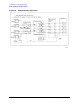
Pulsed-RF IF Signal Path Description
Refer to Figure 6-2, “85102 Pulsed-RF Signal Path,” as you read the following description.
IF Mixer Boards
(A9, A11, A13, A14) The pulsed-RF IF path separates from the normal IF path on
the IF mixer boards. On each IF mixer board the pulsed-RF IF
signal flows through a buffer amplifier to the output connect J5.
A2 Pulse IF MUX Board The pulsed-RF IF signals travel through coaxial cables to the
input of the A2 Pulse IF MUX board. Firmware controlled
switches select either b1 or b2 test IF signals for output at J2,
and either a1 or a2 reference IF signal for output at J6. An
additional function of the A2 purse IF MUX board allows
connection of a 19.9 MHz calibration signal into the test and
reference IF signal paths during IF calibration.
Pulse Detector Boards The test IF signal continues from A2J2 to A3J1 of the A3 Pulse
detector board. The reference IF signal continues from A2J6 to
A4J1 of the A4 Pulse detector board. The detectors on the A3
and A4 boards generate X and Y vector signals from the test and
reference IF signals. A 20 MHz reference signal for the detectors
is supplied by the A6 clock board. The X output is at J2 and the
Y output at J3 on each board.
A16 Remote Application /
Pulse Track and Hold Board The X and Y test signals enter A16 at J3 and J4 respectively.
The X and Y reference signals enter at J1 and J2 respectively.
The signals are fed into track and hold circuits. The outputs of
the T/H circuits are sent on to the A17 Sample/Hold board
multiplexer circuits. At the multiplexer circuits the signal paths
converge to be the same as the normal BW, nonpulsed-RF paths