
User`s guide


184
9
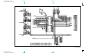
Schematics
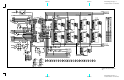
• A1 Earth Referenced Communications Schematic, on page 185
• A1 Main Processor Schematic, on page 186
• A1 Main Gate Array Schematic, on page 187
• A1 Display Controller Schematic, on page 188
• A1 DSP Schematic, on page 189
• A1 Modulation Schematic, on page 190
• A1 System DAC Schematic, on page 191
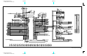
• A1 Timebase Schematic, on page 192
• A1 Phase-Locked Loops Schematic, on page 193
• A1 Trigger Schematic, on page 194
• A1 Clock Divider and Control Schematic, on page 195
• A1 Synthesis IC Schematic, on page 196
• A1 Waveform Memory Schematic, on page 197
• A1 Synchronous Multiplexer Schematic, on page 198
• A1 Digital Waveform and Sync Schematic, on page 199
• A1 Variable-Edge Level Translation Schematic, on page 200
• A1 Waveform DAC, Filters, and Comparator Schematic, on page 201
• A1 Multiplier Schematic, on page 202
• A1 Main Output Circuitry Schematic, on page 203
• A1 Power Supply Schematic, on page 204
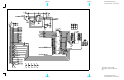
• A2 Keyboard Schematic, on page 205
• A2 Display Schematic, on page 206
• A1 Component Locator (top), on page 207
• A1 Component Locator (bottom), on page 208
• A2 Component Locator (top), on page 209
• A2 Component Locator (bottom), on page 210
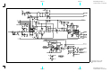
You may notice parts labeled as “No Load” on several of the schematics.
These are parts that were included for design and development but were
later removed to enhance performance or reduce cost.