Service Guide Publication Number 33250-90011 (order as 33250-90100 manual set) Edition 2, March 2003 © Copyright Agilent Technologies, Inc. 2000, 2003 For Safety information, Warranties, and Regulatory information, see the pages following the Index.
Agilent 33250A at a Glance The Agilent Technologies 33250A is a high-performance 80 MHz synthesized function generator with built-in arbitrary waveform and pulse capabilities. Its combination of bench-top and system features makes this function generator a versatile solution for your testing requirements now and in the future.
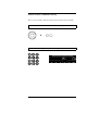
The Front Panel at a Glance 1 2 3 4 5 6 Graph Mode/Local Key Menu Operation Softkeys Waveform Selection Keys Knob Modulation/Sweep/Burst Menus State Storage Menu 7 8 9 10 Utility Menu Instrument Help Topic Menu Output Enable/Disable Key Manual Trigger Key (used for Sweep and Burst only) 11 Cursor Keys Note: To get context-sensitive help on any front-panel key or menu softkey, press and hold down that key.
The Front-Panel Display at a Glance Menu Mode Mode Information Trigger Information Units Output Status Display Icon Numeric Readout Softkey Labels Graph Mode To enter the Graph Mode, press the Parameter Name key. Parameter Value Signal Ground The softkey colors correspond to the waveform parameters.
Front-Panel Number Entry You can enter numbers from the front-panel using one of two methods. Use the knob and arrow keys to modify the displayed number. + Use the numeric keypad and menu softkeys to select the units.
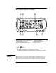
The Rear Panel at a Glance 1 2 3 4 External 10 MHz Reference Input Terminal Internal 10 MHz Reference Output Terminal RS-232 Interface Connector External Modulation Input Terminal 5 Input: External Trig/FSK/Burst Gate Output: Trigger Output 6 GPIB Interface Connector 7 Chassis Ground Use the menu to: • Select the GPIB or RS-232 interface (see chapter 2 in User’s Guide). • Select the GPIB address (see chapter 2 in User’s Guide).
In This Book Specifications Chapter 1 lists the function generator’s specifications. Quick Start Chapter 2 prepares the function generator for use and helps you get familiar with a few of its front-panel features. Front-Panel Menu Operation Chapter 3 introduces you to the frontpanel menu and describes some of the function generator’s menu features. Calibration Procedures Chapter 4 provides calibration, verification, and adjustment procedures for the function generator.
Contents Chapter 1 Specifications 13 Chapter 2 Quick Start To Prepare the Function Generator for Use 21 To Adjust the Carrying Handle 22 To Set the Output Frequency 23 To Set the Output Amplitude 24 To Set a DC Offset Voltage 26 To Set the Duty Cycle 27 To Configure a Pulse Waveform 28 To View a Waveform Graph 29 To Output a Stored Arbitrary Waveform 30 To Use the Built-In Help System 31 To Rack Mount the Function Generator 33 4 Chapter 3 Front-Panel Menu Operation Contents Front-Panel Menu Reference 37
Contents Contents Chapter 4 Calibration Procedures (continued) Calibration Security 68 Calibration Message 70 Calibration Count 70 General Calibration/Adjustment Procedure 71 Aborting a Calibration in Progress 72 Sequence of Adjustments 72 Self-Test 73 Frequency (Internal Timebase) Adjustment 74 Internal ADC Adjustment 75 Output Impedance Adjustment 76 AC Amplitude (high-impedance) Adjustment 78 Low Frequency Flatness Adjustment 80 0 dB Range Flatness Adjustments 81 +10 dB Range Flatness Adjustments 83 +2
Contents Chapter 5 Theory of Operation (continued) Synthesis IC 113 Timebase 115 Phase Locked Loops 116 Clock Divider 118 Trigger and Delay 120 Waveform RAM 122 Synchronous Multiplexer 123 Main Processor 124 Main Gate Array 125 DSP and Gateway 126 Earth-Referenced Logic 126 Front Panel 127 4 Chapter 6 Service Contents Operating Checklist 130 Types of Service Available 131 Repackaging for Shipment 132 Cleaning 132 Electrostatic Discharge (ESD) Precautions 133 Surface Mount Repair 133 Troubleshooting Hin
Contents Contents Chapter 9 Schematics A1 Earth Referenced Communications Schematic 185 A1 Main Processor Schematic 186 A1 Main Gate Array Schematic 187 A1 Display Controller Schematic 188 A1 DSP Schematic 189 A1 Modulation Schematic 190 A1 System DAC Schematic 191 A1 Timebase Schematic 192 A1 Phase-Locked Loops Schematic 193 A1 Trigger Schematic 194 A1 Clock Divider and Control Schematic 195 A1 Synthesis IC Schematic 196 A1 Waveform Memory Schematic 197 A1 Synchronous Multiplexer Schematic 198 A1 Digital
1 1 Specifications
Chapter 1 Specifications Agilent 33250A Function / Arbitrary Waveform Generator 1 WAVEFORMS SIGNAL CHARACTERISTICS Standard Waveforms: Sine, Square, Ramp, Pulse, Noise, Sin(x)/x, Exponential Rise, Exponential Fall, Negative Ramp, Cardiac, DC Volts Arbitrary Waveforms Waveform Length: Amplitude Resolution: Repetition Rate: Sample Rate: Filter Bandwidth: Non-Volatile Memory: 1 to 64K points 12 bits (including sign) 1 µHz to 25 MHz 200 MSa/s 50 MHz Four 64K waveforms 1 FREQUENCY CHARACTERISTICS Sine: Sq
Chapter 1 Specifications Agilent 33250A Function / Arbitrary Waveform Generator OUTPUT CHARACTERISTICS 1 BURST 2 Amplitude (into 50Ω): 10 mVpp to 10 Vpp Accuracy (at 1 kHz, >10 mVpp, Autorange On): ± 1% of setting ±1 mVpp Flatness (sinewave relative to 1 kHz, Autorange On) < 10 MHz: ± 1% (0.1 dB) 3 10 MHz to 50 MHz: ± 2% (0.2 dB) 50 MHz to 80 MHz ± 5% (0.4 dB) Units: Vpp, Vrms, dBm, High Level, Low Level Resolution: 0.1 mV or 4 digits Offset (into 50Ω): ± 5 Vpk ac + dc Accuracy: 1% of setting + 2 mV + 0.
Chapter 1 Specifications Agilent 33250A Function / Arbitrary Waveform Generator 1 SYSTEM CHARACTERISTICS Configuration TImes Function Change Standard: 2 Pulse: Built-In Arb: 2 Frequency Change: Amplitude Change: Offset Change: Select User Arb: Modulation Change: CLOCK REFERENCE (typical) 1 102 ms 660 ms 240 ms 24 ms 50 ms 50 ms < 400 ms for < 16K points < 200 ms Arb Download Times GPIB / RS-232 (115 Kbps) 3 Arb Length Binary ASCII Integer 64K points 23 sec 92 sec 16K points 6 sec 23 sec 8K points 3 sec
Chapter 1 Specifications Agilent 33250A Function / Arbitrary Waveform Generator GENERAL SPECIFICATIONS Power Supply: 100-240 V (±10%) for 50-60 Hz operation, 100-127 V (±10%) for 50-400 Hz operation. IEC 60664 CAT II Power Consumption: 140 VA Operating Environment: 0 °C to 55 °C 80% R.H. to 40 °C Safety Designed to: EN61010-1, CSA1010.
1 Chapter 1 Specifications Agilent 33250A Function / Arbitrary Waveform Generator PRODUCT DIMENSIONS 103.6 mm 254.4 mm 374.0 mm 88.5 mm 216.6 mm 348.3 mm All dimensions are shown in millimeters.
2 2 Quick Start
Quick Start 2 One of the first things you will want to do with your function generator is to become acquainted with the front panel. We have written the exercises in this chapter to prepare the instrument for use and help you get familiar with some of its front-panel operations.
Chapter 2 Quick Start To Prepare the Function Generator for Use To Prepare the Function Generator for Use 1 Check the list of supplied items. 2 Verify that you have received the following items with your instrument. If anything is missing, please contact your nearest Agilent Sales Office. ❑ One power cord. ❑ One User’s Guide. 4 ❑ This Service Guide. ❑ One folded Quick Reference Guide. ❑ Certificate of Calibration. ❑ Connectivity software on CD-ROM. ❑ One RS-232 cable.
Chapter 2 Quick Start To Adjust the Carrying Handle To Adjust the Carrying Handle 2 To adjust the position, grasp the handle by the sides and pull outward. Then, rotate the handle to the desired position.
Chapter 2 Quick Start To Set the Output Frequency To Set the Output Frequency At power-on, the function generator outputs a sine wave at 1 kHz with an amplitude of 100 mV peak-to-peak (into a 50Ω termination). The following steps show you how to change the frequency to 1.2 MHz. 1 Press the “Freq” softkey. 2 4 The displayed frequency is either the power-on value or the frequency previously selected. When you change functions, the same frequency is used if the present value is valid for the new function.
Chapter 2 Quick Start To Set the Output Amplitude To Set the Output Amplitude 2 At power-on, the function generator outputs a sine wave with an amplitude of 100 mV peak-to-peak (into a 50Ω termination). The following steps show you how to change the amplitude to 50 mVrms. 1 Press the “Ampl” softkey. The displayed amplitude is either the power-on value or the amplitude previously selected. When you change functions, the same amplitude is used if the present value is valid for the new function.
Chapter 2 Quick Start To Set the Output Amplitude You can easily convert the displayed amplitude from one unit to another. For example, the following steps show you how to convert the amplitude from Vrms to Vpp. 2 4 Enter the numeric entry mode. Press the key to enter the numeric entry mode. 4 5 Select the new units. Press the softkey that corresponds to the desired units. The displayed value is converted to the new units.
Chapter 2 Quick Start To Set a DC Offset Voltage To Set a DC Offset Voltage 2 At power-on, the function generator outputs a sine wave with a dc offset of 0 volts (into a 50Ω termination). The following steps show you how to change the offset to –1.5 mVdc. 1 Press the “Offset” softkey. The displayed offset voltage is either the power-on value or the offset previously selected. When you change functions, the same offset is used if the present value is valid for the new function.
Chapter 2 Quick Start To Set the Duty Cycle To Set the Duty Cycle Applies only to square waves. At power-on, the duty cycle for square waves if 50%. You can adjust the duty cycle from 20% to 80% for output frequencies up to 25 MHz. The following steps show you how to change the duty cycle to 30%. 4 1 Select the square wave function. Press the key and then set the desired output frequency to any value less than 25 MHz. 2 Press the “Duty Cycle” softkey.
Chapter 2 Quick Start To Configure a Pulse Waveform To Configure a Pulse Waveform 2 You can configure the function generator to output a pulse waveform with variable pulse width and edge time. The following steps show you how to configure a 500 ms pulse waveform with a pulse width of 10 ms and edge times of 50 µs. 1 Select the pulse function. Press the key to select the pulse function and output a pulse waveform with the default parameters. 2 Set the pulse period.
Chapter 2 Quick Start To View a Waveform Graph To View a Waveform Graph In the Graph Mode, you can view a graphical representation of the current waveform parameters. Each softkey parameter is shown in a different color corresponding to the lines above the softkeys at the bottom of the display. Note that the softkeys are listed in the same order as in the normal display mode. 4 1 Enable the Graph Mode. Press the key to enable the Graph Mode.
Chapter 2 Quick Start To Output a Stored Arbitrary Waveform To Output a Stored Arbitrary Waveform 2 There are five built-in arbitrary waveforms stored in non-volatile memory. The following steps show you how to output the built-in “exponential fall” waveform from the front panel. 1 Select the arbitrary waveform function. When you press the key to select the arbitrary waveform function, a temporary message is displayed indicating which waveform is currently selected (the default is “exponential rise”).
Chapter 2 Quick Start To Use the Built-In Help System To Use the Built-In Help System The built-in help system is designed to provide context-sensitive assistance on any front-panel key or menu softkey. A list of help topics is also available to assist you with several front-panel operations. 2 4 1 View the help information for a function key. Press and hold down the key.
Chapter 2 Quick Start To Use the Built-In Help System 3 View the list of help topics. 2 Press the key to view the list of available help topics. To scroll through the list, press the ↑ or ↓ softkey or rotate the knob. Select the third topic “Get HELP on any key” and then press SELECT. Press DONE to exit the help menu. 4 View the help information for displayed messages. Whenever a limit is exceeded or any other invalid configuration is found, the function generator will display a message.
Chapter 2 Quick Start To Rack Mount the Function Generator To Rack Mount the Function Generator You can mount the Agilent 33250A in a standard 19-inch rack cabinet using one of two optional kits available. Instructions and mounting hardware are included with each rack-mounting kit. Any Agilent System II instrument of the same size can be rack-mounted beside the Agilent 33250A. 2 4 Note: Remove the carrying handle, and the front and rear rubber bumpers, before rack-mounting the instrument.
Chapter 2 Quick Start To Rack Mount the Function Generator 2 To rack mount a single instrument, order adapter kit 5063-9240. To rack mount two instruments side-by-side, order lock-link kit 5061-9694 and flange kit 5063-9212. Be sure to use the support rails in the rack cabinet. In order to prevent overheating, do not block the flow of air into or out of the instrument. Be sure to allow enough clearance at the rear, sides, and bottom of the instrument to permit adequate internal airflow.
3 3 Front-Panel Menu Operation
Front-Panel Menu Operation This chapter introduces you to the front-panel keys and menu operation. This chapter does not give a detailed description of every front-panel key or menu operation. It does, however, give you an overview of the frontpanel menus and many front-panel operations. See the Agilent 33250A User’s Guide for a complete discussion of the function generator’s capabilities and operation.
Chapter 3 Front-Panel Menu Operation Front-Panel Menu Reference Front-Panel Menu Reference This section gives an overview of the front-panel menus. The remainder of this chapter shows examples of using the front-panel menus. Configure the modulation parameters for AM, FM, and FSK. • • • • • 4 Select the modulation type. Select an internal or external modulation source. Specify the AM modulation depth, modulating frequency, and modulation shape.
Chapter 3 Front-Panel Menu Operation Front-Panel Menu Reference Store and recall instrument states. • • • • • Store up to four instrument states in non-volatile memory. Assign a custom name to each storage location. Recall stored instrument states. Restore all instrument settings to their factory default values. Select the instrument’s power-on configuration (last or factory default). 3 Configure system-related parameters. • • • • • • • • • • • • • • • Generate a dc-only voltage level.
Chapter 3 Front-Panel Menu Operation To Reset the Function Generator To Reset the Function Generator To reset the instrument to its factory default state, press and then select the Set to Defaults softkey. Select YES to confirm the operation. A complete listing of the instrument’s power-on and reset conditions, 4 see the “Factory Default Settings” table inside the rear cover of this manual.
Chapter 3 Front-Panel Menu Operation To Read the Calibration Information To Read the Calibration Information You can use the instrument’s calibration memory to read the calibration count and calibration message. 3 Calibration Count You can query the instrument to determine how many calibrations have been performed. Note that your instrument was calibrated before it left the factory. When you receive your instrument, read the count to determine its initial value.
Chapter 3 Front-Panel Menu Operation To Unsecure and Secure for Calibration To Unsecure and Secure for Calibration This feature allows you to enter a security code to prevent accidental or unauthorized adjustments of the instrument. When you first receive your instrument, it is secured. Before you can adjust the instrument, you must unsecure it by entering the correct security code. • The security code is set to AT33250A when the instrument is shipped 4 from the factory.
Chapter 3 Front-Panel Menu Operation To Unsecure and Secure for Calibration To Unsecure for Calibration 1 Select the Secure Code interface. Press and then select the Test/Cal softkey. 3 2 Enter the Secure Code. Use the knob to change the displayed character. Use the arrow keys to move to the next character. + When the last character of the secure code is entered, the instrument will be unsecured. 3 Exit the menu. Press the DONE softkey.
Chapter 3 Front-Panel Menu Operation To Unsecure and Secure for Calibration To Secure After Calibration 1 Select the Secure Code interface. Press and then select the Test/Cal softkey. 4 3 2 Enter a Secure Code. Enter up to 12 alphanumeric characters. The first character must be a letter. Use the knob to change the displayed character. Use the arrow keys to move to the next character. + 3 Secure the Instrument. Select the Secure softkey. 4 Exit the menu. Press the DONE softkey.
Chapter 3 Front-Panel Menu Operation To Store the Instrument State To Store the Instrument State You can store the instrument state in one of four non-volatile storage locations. A fifth storage location automatically holds the power-down configuration of the instrument. When power is restored, the instrument can automatically return to its state before power-down. 1 Select the desired storage location. 3 Press and then select the Store State softkey. 2 Select a custom name for the selected location.
Chapter 3 Front-Panel Menu Operation To Configure the Remote Interface To Configure the Remote Interface The instrument is shipped with both a GPIB (IEEE-488) interface and an RS-232 interface. Only one interface can be enabled at a time. The GPIB interface is selected when the instrument is shipped from the factory. 4 3 GPIB Configuration 1 Select the GPIB interface. Press and then select the GPIB softkey from the “I/O” menu. 2 Select the GPIB address.
Chapter 3 Front-Panel Menu Operation To Configure the Remote Interface RS-232 Configuration 1 Select the RS-232 interface. Press and then select the RS-232 softkey from the “I/O” menu. 3 2 Set the baud rate. Press the Baud Rate softkey and select one of the following: 300, 600, 1200, 2400, 4800, 9600, 19200, 38400, 57600 (factory setting), or 115200 baud. 3 Select the parity and number of data bits.
4 4 Calibration Procedures
Calibration Procedures This chapter contains procedures for verification of the instrument’s performance and adjustment (calibration).
Chapter 4 Calibration Procedures Agilent Technologies Calibration Services Closed-Case Electronic Calibration The instrument features closedcase electronic calibration. No internal mechanical adjustments are required. The instrument calculates correction factors based upon the input reference value you set. The new correction factors are stored in non-volatile memory until the next calibration adjustment is performed.
Chapter 4 Calibration Procedures Calibration Interval Calibration Interval The instrument should be calibrated on a regular interval determined by the measurement accuracy requirements of your application. A 1-year interval is adequate for most applications. Accuracy specifications are warranted only if adjustment is made at regular calibration intervals. Accuracy specifications are not warranted beyond the 1-year calibration interval.
Chapter 4 Calibration Procedures Time Required for Calibration Time Required for Calibration The Agilent 33250A can be automatically calibrated under computer control. With computer control you can perform the complete calibration procedure and performance verification tests in approximately 30 minutes once the instrument is warmed-up (see “Test Considerations” on page 54). Manual adjustments and verifications, using the recommended test 4 equipment, will take approximately 2 hours.
Chapter 4 Calibration Procedures Automating Calibration Procedures Automating Calibration Procedures You can automate the complete verification and adjustment procedures outlined in this chapter if you have access to programmable test equipment. You can program the instrument configurations specified for each test over the remote interface. You can then enter readback verification data into a test program and compare the results to the appropriate test limit values.
Chapter 4 Calibration Procedures Recommended Test Equipment Recommended Test Equipment The test equipment recommended for the performance verification and adjustment procedures is listed below. If the exact instrument is not available, substitute calibration standards of equivalent accuracy. Instrument Requirements Recommended Model Use* Digital Multimeter (DMM) ac volts, true rms, ac coupled accuracy: ±0.
Chapter 4 Calibration Procedures Test Considerations Test Considerations For optimum performance, all procedures should comply with the following recommendations: • Assure that the calibration ambient temperature is stable and between 18 °C and 28 °C. Ideally, the calibration should be performed at 23 °C ±1 °C. • Assure ambient relative humidity is less than 80%. • Allow a 1-hour warm-up period before verification or adjustment.
Chapter 4 Calibration Procedures Performance Verification Tests Performance Verification Tests Use the Performance Verification Tests to verify the measurement performance of the instrument. The performance verification tests use the instrument’s specifications listed in the “Specifications” chapter beginning on page 13. You can perform four different levels of performance verification tests: 4 • Self-Test A series of internal verification tests that give high confidence that the instrument is operational.
Chapter 4 Calibration Procedures Performance Verification Tests Self-Test A brief power-on self-test occurs automatically whenever you turn on the instrument. This limited test assures that the instrument is operational. To perform a complete self-test: 1 Press on the front panel. 2 Select the Self Test softkey from the “Test/Cal” menu. A complete description of the self-tests can be found in chapter 6. The instrument will automatically perform the complete self-test procedure when you release the key.
Chapter 4 Calibration Procedures Performance Verification Tests Quick Performance Check The quick performance check is a combination of internal self-test and an abbreviated performance test (specified by the letter Q in the performance verification tests). This test provides a simple method to achieve high confidence in the instrument’s ability to functionally operate and meet specifications. These tests represent the absolute minimum set of performance checks recommended following any service activity.
Chapter 4 Calibration Procedures Performance Verification Tests Amplitude and Flatness Verification Procedures Special Note: Measurements made during the AC Amplitude (highimpedance) Verification procedure (see page 61) are used as reference measurements in the flatness verification procedures (beginning on page 62). Additional reference measurements and calculated references are used in the flatness verification procedures.
Chapter 4 Calibration Procedures Performance Verification Tests Amplitude and Flatness Verification Worksheet 1. Enter the following measurements (from procedure on page 61). 1kHz_0dB_reference = __________________________ Vrms 1kHz_10dB_reference = __________________________ Vrms 1kHz_20dB_reference = __________________________ Vrms 2. Calculate the dBm value of the rms voltages. 1kHz_0dB_reference_dBm = 10 * log(5.0 * 1kHz_0dB_reference2) = 1kHz_10dB_reference_dBm 4 = 10 * log(5.
Chapter 4 Calibration Procedures Internal Timebase Verification Internal Timebase Verification This test verifies the output frequency accuracy of the instrument. All output frequencies are derived from a single generated frequency. 1 Connect a frequency counter as shown below (the frequency counter input should be terminated at 50Ω). 4 2 Set the instrument to the output described in the table below and measure the output frequency. Be sure the instrument output is enabled.
Chapter 4 Calibration Procedures AC Amplitude (high-impedance) Verification AC Amplitude (high-impedance) Verification This procedure checks the ac amplitude output accuracy at a frequency of 1 kHz, and establishes reference measurements for the higher frequency flatness verification procedures. 1 Set the DMM to measure Vrms Volts. Connect the DMM as shown below. 4 4 2 Set the instrument to each output described in the table below and measure the output voltage with the DMM.
Chapter 4 Calibration Procedures Low Frequency Flatness Verification Low Frequency Flatness Verification This procedure checks the AC amplitude flatness at 100 kHz using the reference measurements recorded in the Amplitude and Flatness Verification Worksheet. These measurements also establish an error value used to set the power meter reference. The transfer measurements are made at a frequency of 100 kHz using both the DMM and the power meter. 1 Set the DMM to measure ac Volts.
Chapter 4 Calibration Procedures 0 dB Range Flatness Verification 0 dB Range Flatness Verification This procedure checks the high frequency ac amplitude flatness above 100 kHz on the 0 dB attenuator range. 1 Connect the power meter to measure the output amplitude of the instrument as shown below. 4 4 2 Set the power meter reference level to equal 100kHz_0dB_offset. This sets the power meter to directly read the flatness error specification.
Chapter 4 Calibration Procedures 0 dB Range Flatness Verification 3 Set the instrument to each output described in the table below and measure the output amplitude with the power meter. Press to set the output impedance to 50Ω. Be sure the output is enabled. Agilent 33250A Output Setup Q 4 Q Q Q Measurement Function Amplitude Frequency Nominal Error 50 Ω Sine Wave +3.51 dBm 100.000 kHz 0 dB ± 0.086 dB 50 Ω Sine Wave +3.51 dBm 200.000 kHz 0 dB ± 0.086 dB 50 Ω Sine Wave +3.
Chapter 4 Calibration Procedures +10 dB Range Flatness Verification +10 dB Range Flatness Verification This procedure checks the high frequency ac amplitude flatness above 100 kHz on the +10 dB attenuator range. 1 Connect the power meter to measure the output amplitude of the instrument as shown on page 63. 2 Set the power meter reference level to equal to the calculated 100kHz_10dB_offset value. This sets the power meter to directly read the flatness error specification.
Chapter 4 Calibration Procedures +20 dB Range Flatness Verification +20 dB Range Flatness Verification This procedure checks the high frequency ac amplitude flatness above 100 kHz on the +20 dB attenuator range. 1 Connect the power meter to measure the output voltage of the instrument as shown below. 4 2 Set the power meter reference level to equal to the calculated 100kHz_20dB_offset value. This sets the power meter to directly read the flatness error specification.
Chapter 4 Calibration Procedures +20 dB Range Flatness Verification 3 Set the instrument to each output described in the table below and measure the output amplitude with the power meter. Press to set the output impedance to 50Ω. Be sure the output is enabled Agilent 33250A Output Setup Q Q Q Q Measurement Function Amplitude Frequency Nominal Error 50 Ω Sine Wave +23.90 dBm 100.000 kHz 0 dB ± 0.086 dB 50 Ω Sine Wave +23.90 dBm 200.000 kHz 0 dB ± 0.086 dB 50 Ω Sine Wave +23.
Chapter 4 Calibration Procedures Calibration Security Calibration Security This feature allows you to enter a security code to prevent accidental or unauthorized adjustments of the instrument. When you first receive your instrument, it is secured. Before you can adjust the instrument, you must unsecure it by entering the correct security code. See “To Unsecure and Secure for Calibration”, on page 41 for a procedure to enter the security code.
Chapter 4 Calibration Procedures Calibration Security To Unsecure the Instrument Without the Security Code To unsecure the instrument without the correct security code, follow the steps below. See “To Unsecure and Secure for Calibration” on page 41. See “Electrostatic Discharge (ESD) Precautions” on page 133 before beginning this procedure. 1 Disconnect the power cord and all input connections. 2 Remove the instrument cover. See “Disassembly” on page 140. 4 3 Remove the main power supply.
Chapter 4 Calibration Procedures Calibration Message Calibration Message The instrument allows you to store one message in calibration memory. For example, you can store such information as the date when the last calibration was performed, the date when the next calibration is due, the instrument’s serial number, or even the name and phone number of the person to contact for a new calibration. You can record a calibration message only from the remote interface and only when the instrument is unsecured.
Chapter 4 Calibration Procedures General Calibration/Adjustment Procedure General Calibration/Adjustment Procedure The following procedure is the recommended method to complete an instrument calibration. This procedure is an overview of the steps required for a complete calibration. Additional details for each step in this procedure are given in the appropriate sections of this chapter. 4 1 Read “Test Considerations” on page 54. 2 Unsecure the instrument for calibration (see page 68).
Chapter 4 Calibration Procedures Aborting a Calibration in Progress Aborting a Calibration in Progress Sometimes it may be necessary to abort a calibration after the procedure has already been initiated. You can abort a calibration at any time by turning off the power. When performing a calibration from the remote interface, you can abort a calibration by issuing a remote interface device clear message followed by a *RST. The instrument stores calibration constants at the end of each adjustment procedure.
Chapter 4 Calibration Procedures Self-Test Self-Test Self-Test is performed as the first step to ensure the instrument is in working order before beginning any additional adjustments. 1 Press on the front panel. Select Perform Cal on the “Test / Cal” menu. Enter setup number “1” and select BEGIN. 4 Setup 1 Performs the Self-test. The Main Output is disabled during test. 2 If the instrument fails any self-test, you must repair the instrument before continuing the adjustment procedures.
Chapter 4 Calibration Procedures Frequency (Internal Timebase) Adjustment Frequency (Internal Timebase) Adjustment The function generator stores a calibration constant that sets the TCXO to output exactly 10 MHz. 1 Set the frequency counter resolution to better than 0.1 ppm and the input termination to 50Ω (if your frequency counter does not have a 50Ω input termination, you must provide an external termination). Make the connections shown below.
Chapter 4 Calibration Procedures Internal ADC Adjustment Internal ADC Adjustment The function generator stores calibration constants related to the gain and offset of the internal ADC. Setup 6 must always be performed before any other adjustments are attempted. The internal ADC is then used as a source for the calibration constants generated in setup 7. 1 Make the connections as shown below. 4 Modulation In 4 2 Set the DMM to display 5½ digits and measure the dc value. Record the measurement.
Chapter 4 Calibration Procedures Output Impedance Adjustment 5 Enter and begin the following setup. Setup 7* Self-calibration. The Main Output is disabled during test. * Constants are stored after completing this setup. 6 There are no specific operational verification tests for setups 6 and 7 since the constants generated affect almost all behavior of the instrument. Continue with the next adjustment procedure in this chapter.
Chapter 4 Calibration Procedures Output Impedance Adjustment 2 Use the DMM to make a resistance measurement at the front panel Output connector for each setup in the following table. The expected measured value is approximately 50Ω.
Chapter 4 Calibration Procedures AC Amplitude (high-impedance) Adjustment AC Amplitude (high-impedance) Adjustment The function generator stores a calibration constant for each highimpedance attenuator path. The gain coefficient of each path is calculated using two measurements; one with the waveform DAC at the + output and one with waveform DAC at the – output. The setups, therefore, must be performed in pairs. 1 Connect the DMM as shown below.
Chapter 4 Calibration Procedures AC Amplitude (high-impedance) Adjustment 2 Use the DMM to measure the dc voltage at the front-panel Output connector for each setup in the following table. Nominal Signal Setup DC level 18 +0.015 V Output of -30 dB range 19* -0.015 V Output of -30 dB range 20 +0.05 V Output of -20 dB range 21* -0.05 V Output of -20 dB range 22 +0.15 V Output of -10 dB range 23* -0.15 V Output of -10 dB range 24 +0.50 V Output of 0 dB range 25* -0.
Chapter 4 Calibration Procedures Low Frequency Flatness Adjustment Low Frequency Flatness Adjustment The Low Frequency Flatness adjustment calculates the flatness response of 3 attenuator paths with the Elliptical filter and 2 attenuator paths with the Linear Phase filter. 1 Set the DMM to measure Vrms. Make the connections shown on page 78. 2 Use the DMM to measure the output voltage for each of the setups in the table below. Nominal Signal 4 Setup Frequency Amplitude 34* 1 kHz 0.
Chapter 4 Calibration Procedures 0 dB Range Flatness Adjustments 0 dB Range Flatness Adjustments 1 Connect the power meter as shown on page 83. 2 Use the power meter to measure the output amplitude for each of the setups in the table below. 4 Setup 44 establishes the power meter reference for all the remaining setups in this table. You must always perform setup 44 before any of the following setups. Note Nominal Signal 4 Setup Frequency Amplitude 44* 100 kHz 0.
Chapter 4 Calibration Procedures 0 dB Range Flatness Adjustments Nominal Signal 4 Setup Frequency Amplitude 58* 200 kHz 0.28 Vrms 2 dBm Flatness for 0 dB, Linear Phase 59* 500 kHz 0.28 Vrms 2 dBm Flatness for 0 dB, Linear Phase 60* 1.5 MHz 0.28 Vrms 2 dBm Flatness for 0 dB, Linear Phase 61* 5 MHz 0.28 Vrms 2 dBm Flatness for 0 dB, Linear Phase 62* 10.1 MHz 0.28 Vrms 2 dBm Flatness for 0 dB, Linear Phase 63* 25.1 MHz 0.28 Vrms 2 dBm Flatness for 0 dB, Linear Phase 64 25.
Chapter 4 Calibration Procedures +10 dB Range Flatness Adjustments +10 dB Range Flatness Adjustments Note The Linear Phase path is not adjusted. It is approximated using the other path’s values. 1 Connect the power meter as shown below. 4 4 2 Use the power meter to measure the output amplitude for each of the setups in the table on the next page. Note Setup 66 establishes the power meter reference for all the remaining setups in this table.
Chapter 4 Calibration Procedures +10 dB Range Flatness Adjustments Nominal Signal 4 Setup Frequency Amplitude 66* 100 kHz 0.9 Vrms 12 dBm Power Meter Reference for +10 dB Range 67* 200 kHz 0.9 Vrms 12 dBm Flatness for +10 dB, Elliptical Filter 68* 500 kHz 0.9 Vrms 12 dBm Flatness for +10 dB, Elliptical Filter 69* 1.5 MHz 0.9 Vrms 12 dBm Flatness for +10 dB, Elliptical Filter 70* 5 MHz 0.9 Vrms 12 dBm Flatness for +10 dB, Elliptical Filter 71* 10.1 MHz 0.
Chapter 4 Calibration Procedures +20 dB Range Flatness Adjustment +20 dB Range Flatness Adjustment Most power meters will require an attenuator (-20 dB) or special power head to measure the +20 dB output. Caution Be sure to correct the measurements for the specifications of the attenuator you use. For example, if the nominal attenuator value is –20 dB at the specified frequency, you must add 20 dB to the power meter reading before entering the value. 4 1 Make the connections as shown below.
Chapter 4 Calibration Procedures +20 dB Range Flatness Adjustment Nominal Signal 4 Setup Frequency Amplitude 84* 5 MHz 2.8 Vrms 22 dBm Flatness for +20 dB, Elliptical Filter 85* 10.1 MHz 2.8 Vrms 22 dBm Flatness for +20 dB, Elliptical Filter 86* 25.1 MHz 2.8 Vrms 22 dBm Flatness for +20 dB, Elliptical Filter 87* 40.1 MHz 2.8 Vrms 22 dBm Flatness for +20 dB, Elliptical Filter 88* 50.1 MHz 2.8 Vrms 22 dBm Flatness for +20 dB, Elliptical Filter 89* 60.1 MHz 2.
Chapter 4 Calibration Procedures Pulse Width (Trailing Edge Delay) Adjustment Pulse Width (Trailing Edge Delay) Adjustment The function generator stores calibration constants used to set the trailing edge delay (see the discussion on page 110). These setups place the instrument in pulse mode (at 8 MHz). Setup 102 must be performed immediately prior to setup 103. 1 Set the oscilloscope to use averaging to determine the pulse width.
Chapter 4 Calibration Procedures Pulse Edge Time Adjustment Pulse Edge Time Adjustment The function generator stores calibration constants used to calculate the slope and offset of the edge time DAC outputs. These setups output 100 Hz pulses with 5 ms pulse widths. The setups, following the first three, must be done in pairs (i.e., 107 immediately before 108).
Chapter 4 Calibration Procedures Duty Cycle Adjustment Duty Cycle Adjustment The function generator stores a calibration constant used to calculate the square wave duty cycle. This setup outputs a 25.1 MHz square wave. The output frequency in this procedure is chosen to avoid artifacts of DDS signal generation and internal clock frequencies. The “Internal ADC Adjustment”, on page 75 must be completed before 4 doing this procedure.
Chapter 4 Calibration Procedures Output Amplifier Adjustment (Optional) Output Amplifier Adjustment (Optional) This adjustment should only be performed if repairs have been made the output amplifier circuitry (U1903, U1904, and associated components). This adjustment is performed at the factory and re-adjustment is not needed or recommended. Note You must perform a complete calibration of the instrument following this adjustment. 1 Disconnect the power cord and all input connections.
Chapter 4 Calibration Procedures Calibration Errors Calibration Errors The following errors are failures that may occur during a calibration. System error messages are described in chapter 5 of the Agilent 33250A User’s Guide. Self-test error messages are described in this manual beginning on page 137.
4 92
5 5 Theory of Operation
Theory of Operation This chapter provides descriptions of the circuitry shown on the schematics in chapter 9.
Chapter 5 Theory of Operation Block Diagram Block Diagram A block diagram is shown on the next page. The function generator’s circuits may be divided into three main categories: power supplies, analog circuits, and digital circuits. Each portion of the block diagram is described in the following sections. The line input voltage is filtered, and then applied to the main power supply. The main power supply provides all power to the instrument. Secondary power supplies are contained on the main circuit board.
Agilent 33250A Block Diagram 5 96
Chapter 5 Theory of Operation Main Power Supply Power Supplies The line input voltage is filtered, and then applied to the main power supply. The main power supply provides all power to the instrument. Secondary power supplies are contained on the main circuit board. The secondary supplies control the fan, create the –2.1 V and +3.3 V voltages, and provide the isolated +5 V supply. 4 Main Power Supply The main power supply is a switching supply.
Chapter 5 Theory of Operation On-Board Power Supplies On-Board Power Supplies See “A1 Power Supply Schematic” on page 204. The on-board power supply controls the on/off state of the power supply and conditions the main supplies for use by the analog and digital circuits. Over-temperature protection is also provided. The main supply provides a +12 V standby power supply that is used by the power on/off circuitry. The electronic power switch is controlled by the PWR_SWITCH* line.
Chapter 5 Theory of Operation On-Board Power Supplies The variable-speed fan is driven by a temperature-controlled switching regulator which is powered by +12V_ER. Comparator U2002-A is configured as an oscillator whose output (at C2013) is a triangle wave. Thermistor R2016 senses the incoming air temperature and U2001-A converts it to a voltage. U2002-B compares this voltage to the triangle wave and outputs a square wave whose duty cycle varies with temperature.
Chapter 5 Theory of Operation Waveform DAC and Filters Analog Circuitry The analog circuitry begins at the Waveform DAC and continues to the main output. Sine, ramp, noise, and arbitrary waveforms pass directly from the Waveform DAC to the main output circuitry. Square waves and pulses are formed in the digital waveform and variable-rate level translation circuits. Waveform DAC and Filters See “A1 Waveform DAC, Filters, and Comparator Schematic” on page 201.
Chapter 5 Theory of Operation Digital Waveform, Pulse, and Sync U1704 is a comparator driven by the 2.2 Vp-p signal from U1703 to generate square waves. System DAC signal, V_THRESH, sets the duty cycle of the square wave. The square wave output, SQUARE_DWF, is sent to the SYNC selector (U1502) and the AND gate U1507-B where, if it is enabled by SQUARE_DWF_EN being high, it is passed to the Digital Waveform Translator.
Chapter 5 Theory of Operation Digital Waveform, Pulse, and Sync LE and TE are outputs from register U1504 which is clocked differentially by WFDAC_CLK±. The pulse period always consists of an integral number of clocks; the clock frequency is controlled to achieve fine period resolution. The pulse itself consists of a number of clocks plus the delay provided by the delay circuit; fine control of the pulse width is achieved by varying the delay via a control voltage, V_TEDLY.
Chapter 5 Theory of Operation Digital Waveform, Pulse, and Sync U1508-D sets the current in Q1501 (from 0 to 60 µA) according to the voltage difference between V_TEDLY and VREF (as buffered by U1508-A). This current is converted to U1506-A’s threshold voltage (approximately –0.8 V to –1.4 V) by U1508-B. Multiplexer U1502 selects which signal is put out at the SYNC connector, depending on the states of SYNC_CTL0 and SYNC_CTL1 from the Synthesis IC.
Chapter 5 Theory of Operation Digital Waveform Translator Digital Waveform Translator See “A1 Variable-Edge Level Translation Schematic” on page 200. Digital Waveform Translator converts the square or pulse waveform’s (DWFe) ECL levels to the ±1 V levels required by Amplitude Multiplier. It also sets the rise and fall time of the square wave or pulse. The input signal, DWFe, is amplified and level translated to ±640 mV by clamping amplifier U1602. Clamping levels are set by R1613, R1616, R1628, and R1631.
Chapter 5 Theory of Operation Digital Waveform Translator Edge speed range is set by TR_RNG(4:1) which control transistors Q1603 through Q1606. If a transistor is off, the associated integrating capacitor (C1610 through C1613) floats and is effectively out of the circuit. If a transistor is on, however, one end of the its capacitor is grounded and capacitor is switched into the circuit. U1602 converts the –0.8 V to –1.6 V to ±0.64 V levels. The upper clamp voltage of –1.
Chapter 5 Theory of Operation Amplitude Multiplier Amplitude Multiplier See “A1 Multiplier Schematic” on page 202. Latching relay K1801 selects either the analog waveform, AWF, or the digital waveform, DWF, for application to multiplier U1801. K1801 is controlled by SET_AWF and SET_DWF from U306. The amplitude multiplier provides approximately 10 dB of fine control to the instrument’s output amplitude, interpolating between attenuator steps. The multiplier also performs AM modulation.
Chapter 5 Theory of Operation Main Output Circuitry Main Output Circuitry See “A1 Main Output Circuitry Schematic” on page 203. The main output circuitry attenuates or amplifies the waveform to its final amplitude level and adds any dc offset required. The output is also protected against harmful combinations of load impedance and output voltage. 4 0 dB path is shown 5 R1915, R1917, and R1918 form a –10 dB attenuator that is switched by K1901.
Chapter 5 Theory of Operation Main Output Circuitry Attenuators and/or the amplifier are switched in to set the output amplitude range according to the following table: Offset < 1 V Amplitude Range (Vpp into 50Ω) –10 dB –20 dB Amp –10 dB –20 dB Amp In In Out N/A N/A N/A 30 mV to 100 mV Out In Out N/A N/A N/A 96 mV to 316 mV In Out Out In In In Out Out Out Out In In In Out In In Out In Out Out In Out Out In < 31.6 mV 300 mV to 1 V 0.96 V to 3.
Chapter 5 Theory of Operation Main Output Circuitry Non-latching relays K1904 and K1905 switch a 100-MHz, 5th-order, low-pass filter (L1907 through L1909 and C1923 through C1926) into the signal path to reduce high-frequency distortion on continuous sine waves. If the instrument is off, if the output has been disabled, or if the output protection circuitry has been activated, the coils of both relays are de-energized and the main output is disconnected from the rest of the instrument.
Chapter 5 Theory of Operation System ADC System ADC See “A1 Modulation Schematic” on page 190. Modulation by an external source, both AM and FM, is performed digitally by sampling the external input at the modulation BNC, adjusting the data to match the current modulation specification (deviation in FM, depth in AM). The sampled data are sent to the DSP which applies the resulting data to the waveform generation hardware. The sample rate is 468.75 kHz.
Chapter 5 Theory of Operation System ADC U603 is the final stage of a multiplexer used to select the ADC input source. The rear panel modulation input is applied directly to one of the multiplexer inputs for the ±1 V input range, and through divider R618 and R620 for the ±5 V input range. Other U603 inputs include ground, +1.25 V (VREF_d2), MEAS_OA_ADJ from U1903, and three MEAS lines, each of which are multiplexed signals from the first stage multiplexers U706, U707, and U708.
Chapter 5 Theory of Operation System DAC System DAC See “A1 System DAC Schematic” on page 191. The System DAC provides dc voltages that control various parameters of the instrument’s operation. This schematic page also includes analog multiplexers that select various signals for measurement by the A/D Converter. The System DAC U701 is loaded with serial data from the Main Gate Array, U302, using SYSDAC_CLK, SYSDAC_STRB*, and SYSDAC_DATA. The DAC’s voltage reference is 2.
Chapter 5 Theory of Operation Synthesis IC Digital Circuitry The digital circuitry contains all the waveform generation circuitry and waveform memory. The main CPU and communications CPU (outguard) are also included. 4 Synthesis IC See “A1 Synthesis IC Schematic” on page 196. U1201 is an SRAM-based field-programmable gate array that implements most of the logic for waveform generation.
Chapter 5 Theory of Operation Synthesis IC DDS Behavior DDS waveform generation begins with a high-resolution phase accumulator. The most significant phase bits are interpolated into four waveform address streams. These four address streams are then interleaved into two streams at twice the rate. These two streams become the A_EVN and A_ODD waveform address lines.
Chapter 5 Theory of Operation Timebase Timebase See “A1 Timebase Schematic” on page 192. The Timebase provides a 10 MHz clock from which all the waveform generation timing signals are ultimately derived. This clock can have one of two sources: the internal crystal oscillator (U803) or an External BNC input connector. 4 U803’s frequency is controlled by the System DAC signal, V_TBCAL. When an external timebase is used, EXT_TB_EN is asserted, turning Q801 and U803 off.
Chapter 5 Theory of Operation Phase Locked Loops Phase Locked Loops See “A1 Phase-Locked Loops Schematic” on page 193. There are two phase locked loops (PLLs). A primary PLL, which ultimately furnishes the clocks for DDS waveforms, and a triggered PLL, which is used in pulse generation. The primary PLL multiplies the 10 MHz frequency reference to 800 MHz. The PLL synthesizer, U901, is programmed at power on using the serial transfer lines PRI_DATA, PRI_DCLCK, and PRI_STRB from the Main Processor U202.
Chapter 5 Theory of Operation Phase Locked Loops The triggered PLL synthesizer, U904, drives U905 which shifts and scales the output voltage to match the input requirements of varactor CR901. U907 is a programmable delay, fed back upon itself through a differential RC network (the capacitance of CR901, resistors R929 and R930, and gate U906). U907 is programmed through the VCO(6:0) lines from the Synthesizer IC.
Chapter 5 Theory of Operation Clock Divider Clock Divider See “A1 Clock Divider and Control Schematic” on page 195. U1101 divides the 800 MHz clock from U903 by two, producing a differential 400 MHz clock signal, CLKx2±. TRIG_SYNC from the Trigger Delay circuits goes high briefly when the instrument is triggered, disabling this divider for a short time to synchronize the synthesizer with the trigger.
Chapter 5 Theory of Operation Clock Divider One half of U1109-A divides LOGIC_CLK by two to create the 100 MHz signal, CLK_d2e. The other half of U1109-A divides CLK_d2e by two to create a 50 MHz signal that is delayed by 2.5 ns in U1110 to become CLK_d4e. CLK_d2e* is gated by U1107-A and U1107-B, then re-clocked by U1109-B to form two 100 MHz clocks, CLK_d2_ODDe and CLK_d2_EVNe, that can be individually disabled by negating either CLK_EN_ODD or CLK_EN_EVN.
Chapter 5 Theory of Operation Trigger and Delay Trigger and Delay See “A1 Trigger Schematic” on page 194. The instrument has a bi-directional, chassis referenced, TTL trigger BNC connector. Triggering can occur either from the external trigger BNC input or from the instrument’s internal trigger. The user can elect to send the instrument’s internal trigger out the trigger BNC connector to synchronize other instruments. External trigger inputs are buffered by U1002-A and applied to the opto-isolator U1003.
Chapter 5 Theory of Operation Trigger and Delay Assuming the synthesizer is stopped and triggers enabled, TRIG_ARM will be high. A rising edge on TRIGe will then clock a “1” into flip-flop U1007, causing U1008 pin 2 to go “low”, and allowing C1007 to begin charging in a negative direction through R1049. TRIG_SYNC is also asserted at this time to disable the synthesizer clocks.
Chapter 5 Theory of Operation Waveform RAM Waveform RAM See “A1 Waveform Memory Schematic” on page 197. There are two banks of waveform RAM, referred to as “ODD” (U1305) and “EVEN” (U1304). These RAMs perform all operations synchronously. When writing, address and data are clocked into input latches and then stored in the memory by on-chip self-timed circuitry. When reading, address is latched on one clock edge and data is clocked out on the next clock edge. U1304 and U1305 have two clock sources.
Chapter 5 Theory of Operation Synchronous Multiplexer Synchronous Multiplexer See “A1 Synchronous Multiplexer Schematic” on page 198. Waveform data from the Waveform RAM is converted from TTL levels to ECL levels using resistive dividers (R1402 through R1413, R1417 through R1428, R1437 through R1448, and R1455 through R1466). The control signals from U1202 are converted from TTL to ECL by 4 U1402 and U1403. U1404 through U1407 form a pipeline stage clocked at 100 MHz by CLK_d2e.
Chapter 5 Theory of Operation Main Processor Main Processor See “A1 Main Processor Schematic” on page 186. U202 is the main CPU for the instrument. U214 provides the 18 MHz clock for the main CPU.
Chapter 5 Theory of Operation Main Gate Array Main Gate Array See “A1 Main Gate Array Schematic” on page 187. U302 is a Field-Programmable Gate Array. When RESET* is asserted, U301 serially loads the gate array with its contents. U302 asserts MAR_AWAKE* to indicate to the CPU that it is loaded and ready. The Main Gate Array performs many functions within the instrument 4 including: • Main CPU address decoding and bus handshaking.
Chapter 5 Theory of Operation DSP and Gateway DSP and Gateway See “A1 DSP Schematic” on page 189. U506 is the digital signal processor. It is clocked at 40.96 MHz from U505. The DSP RAM, U507, is loaded by the Main CPU through the gateway. U506 also communicates with the main CPU via a serial connection, assisted by U302. The bus gateway is controlled by the Main CPU U302.
Chapter 5 Theory of Operation Front Panel Front Panel See “A2 Keyboard Schematic” on page 205 and “A2 Display Schematic” on page 206. The front panel contains a keyboard, a liquid crystal display (LCD), a piezoelectric speaker, and a rotary encoder. The keyboard is arranged in five columns and eight rows. The keys are4 scanned one column at a time. Some of the keys have an LED incorporated into the key to indicate the instrument’s operating state. U301 scans the columns and reads the key presses.
5 128
6 6 Service
Service This chapter discusses the procedures involved for returning a failed instrument to Agilent Technologies for service or repair.
Chapter 6 Service Types of Service Available Types of Service Available If your instrument fails during the warranty period (within three years of original purchase), Agilent Technologies will replace or repair it free of charge. After your warranty expires, Agilent will replace or repair it at a competitive price. The standard repair process is “whole unit exchange”. The replacement units are fully refurbished and are shipped with new 4 calibration certificates.
Chapter 6 Service Repackaging for Shipment Repackaging for Shipment If the unit is to be shipped to Agilent for service or repair, be sure to: • Attach a tag to the unit identifying the owner and indicating the required service or repair. Include the model number and full serial number. • Place the unit in its original container with appropriate packaging material for shipping. • Secure the container with strong tape or metal bands.
Chapter 6 Service Electrostatic Discharge (ESD) Precautions Electrostatic Discharge (ESD) Precautions Almost all electrical components can be damaged by electrostatic discharge (ESD) during handling. Component damage can occur at electrostatic discharge voltages as low as 50 volts. The following guidelines will help prevent ESD damage when servicing the instrument or any electronic device. 4 • Disassemble instruments only in a static-free work area. • Use a conductive work area to reduce static charges.
Chapter 6 Service Troubleshooting Hints Troubleshooting Hints This section provides a brief check list of common failures. Before troubleshooting or repairing the instrument, make sure the failure is in the instrument rather than any external connections. Also make sure that the instrument is accurately calibrated within the last year (see “Calibration Interval”, on page 50). The instrument’s circuits allow troubleshooting and repair with basic equipment such as a 6½ digit multimeter.
Chapter 6 Service Troubleshooting Hints Power Supplies Verify the power supplies generated on the A1 board. WARNING Shock Hazard. To check the power supplies, remove the instrument cover as described in “Disassembly”, on page 140. Be sure to use the correct ground point when checking the supplies. 4 The power supply voltages are tabulated below. Power Supply Minimum Maximum +12v_ER 11.4 V 12.6 V +5V_ER 4.75 V 5.25 V –5.2 V –5.46 V –4.94 V –16 V –16.8 V –15.2 V +16 V 15.2 V 16.8 V +5.
Chapter 6 Service Self-Test Procedures Self-Test Procedures Power-On Self-Test Each time the instrument is powered on, a small set of self-tests are performed. These tests check that the minimum set of logic and output hardware are functioning properly. The power-on self test consists of tests 601 through 606. Complete Self-Test To perform a complete self-test: 1 Press on the front panel. 2 Select the Self Test softkey from the “Test / Cal” menu.
Chapter 6 Service Self-Test Procedures Self-Tests A complete self-test performs the following tests. A failing test is indicated by the test number and description in the display. 601 System logic failed This test performs a write/readback test on the two control registers (Control Register 1 and Control Register 2/Keyboard Readback) the main 4 logic FPGA, U302. Failure of this test indicates that the main CPU (U202) can’t communicate with the main logic FPGA (U301).
Chapter 6 Service Self-Test Procedures 607 - 614 Power supplies failed This test uses the internal ADC to measure the voltages of the internal power supplies. A failure means one or more of the power supplies measured outside the expected range. The error numbers and their corresponding power supplies are listed below. 607: 608: 609: 610: 611: 612: 613: 614: 6 Ground +16 +12V +5V +3.3V -2.1V -5.
Chapter 6 Service Self-Test Procedures 618 - 625 System DAC failed These tests use the internal ADC (U1701) to verify that the system DACs are working correctly. There are eight system DACs. For each DAC, ADC readings are taken at 25%, 50%, and 75% of full scale. The delta between ADC readings are compared to the delta of DAC values to make sure the DAC outputs scale proportionally to the inputs. A failure indicates a malfunctioning system DAC(s), sysDac Mux channel(s) circuit, or ADC Mux channel(s).
Chapter 6 Service Disassembly Disassembly The following tools are recommended for disassembly. • T15 Torx® driver (all screws) • 11 mm nut driver (front-panel disassembly) • 14 mm nut driver (rear-panel BNC connectors) • 5 mm nut driver (rear-panel RS-232 connector) • #1 Pozi-Drive (for display assembly) WARNING SHOCK HAZARD. Only service-trained personnel who are aware of the hazards involved should remove the instrument covers.
Chapter 6 Service Disassembly General Disassembly Procedure 1 Turn off the power. Remove all cables from the instrument. 2 Rotate the handle upright and pull off. 4 3 Pull off the instrument bumpers. 6 4 Loosen the two captive screws in the rear bezel and remove the rear bezel.
Chapter 6 Service Disassembly 5 Remove the screw in the bottom of the instrument cover. Slide off the cover. Slide Cover Off Remove screw 6 Remove the screw securing the top shield. Slide the shield back and then up to lift off. The A3 power supply assembly is attached to the top shield.
Chapter 6 Service Disassembly 7 Lay the top shield and power supply assembly to the side. 4 Many of the service procedures can now be performed without further disassembly. Troubleshooting and service procedures that require power be applied can be performed with the instrument in this state of disassembly. WARNING SHOCK HAZARD. Only service-trained personnel who are aware of the hazards involved should remove the instrument covers.
Chapter 6 Service Disassembly Removing the Main Power Supply Assembly Disconnect the ribbon cable and the power cable. The main power supply should be replaced as an assembly. Remove the four screws to remove the power supply assembly from the top shield and safety shield. Be sure to retain the top shield and safety shield for re-use. Front-Panel Removal Procedure 1 Turn the unit over. Remove the bottom shield screw and bottom shield.
Chapter 6 Service Disassembly 2 Pull up to remove the Sync and Output cable from the cable clip. Disconnect the Sync and Output cable from the main board. Pull up the clamp and disconnect the front panel ribbon cable from the main board. Cable Clip 4 Ribbon Cable 3 Remove the two screws holding the front edge of the A1 assembly to the chassis.
Chapter 6 Service Disassembly 4 There should now be enough play in the chassis sides and front panel plastic to allow the side of the front panel to be disconnected from the chassis. Remove the right side first as shown.
Chapter 6 Service Disassembly Front-Panel Disassembly 1 Remove the captive screw holding the safety shield. Carefully pry the RFI shield clips out of the slots in the safety shield and remove the safety shield. RFI Clip 4 Captive Screw RFI Clip 2 Unplug the inverter cable on the display assembly. Lift up the clamp and unplug the ribbon cable. Lift out the display assembly.
Chapter 6 Service Disassembly 3 Remove the knob. Remove the nut holding the rotary encoder to the front-panel. Lift out the A2 assembly.
Chapter 6 Service Disassembly Removing and Replacing the Fan The fan is held in place by four custom vibration-reducing fasteners. To remove the fan, disconnect the fan cable from the A1 assembly. Pry up and pull out the center tab of the fasteners.
Chapter 6 Service Disassembly 6 150
7 Replaceable Parts 7
Replaceable Parts This chapter contains information for ordering replacement parts for your instrument. The parts lists are divided into the following sections. • 33250-66511 – Main PC Assembly (A1), on page 153 • 33250-66502 – Front-Panel PC Assembly (A2), on page 176 • 33250A Chassis Assembly, on page 177 • 33250-60201 – Front-Panel Assembly, on page 178 • Manufacturer’s List, on page 179 Parts are listed in alphanumeric order according to their schematic reference designators.
Chapter 7 Replaceable Parts 33250-66511 – Main PC Assembly (A1) 33250-66511 – Main PC Assembly (A1) Reference Designator Agilent Part Qty Number C101 - C102 C103 C104 - C107 C108 C109 C110 - C113 C114 C115 - C125 C201 0160-7798 0160-5947 0160-7736 0160-5961 0160-5957 0160-7736 0180-4918 0160-7798 0160-7798 C202 C203 - C205 C206 - C229 C301 - C323 C401 C402 C403 C404 C405 C406 0160-5947 0160-7736 0160-7798 0160-7798 0160-5947 0160-7061 0180-3751 0160-7736 0180-4577 0160-7798 C407 C408 C409 - C413 C501
Chapter 7 Replaceable Parts 33250-66511 – Main PC Assembly (A1) Reference Designator 7 Agilent Part Qty Number C622 C623 C624 C625 C626 C627 C628 C629 C630 C631 - C632 0160-7061 0160-7736 0160-7798 0160-7736 0160-5945 0160-7798 0160-6444 0160-7061 0160-7798 0160-7736 C701 - C703 C704 C705 C706 C707 C708 C709 - C718 0160-7798 0160-7736 0160-5945 0160-5975 0160-7798 0160-7736 0160-7798 C801 C802 - C804 C805 C806 - C808 C809 C810 C811 C812 - C813 C814 C815 0180-4758 0160-7736 0180-4577 0160-7798 0160-
Chapter 7 Replaceable Parts 33250-66511 – Main PC Assembly (A1) Reference Designator Agilent Part Qty Number C920 C921 C922 - C923 C924 - C925 C926 C1001 - C1002 C1003 C1004 - C1005 C1006 C1007 0160-5945 0160-7707 0160-7798 0160-5945 0160-7798 0160-7798 0160-5947 0160-7798 0160-5957 0160-7721 1 C1008 C1009 C1010 C1011 C1012 C1013 C1014 C1015- C1017 C1018 - C1019 C1020 - C1025 0160-7708 0160-7736 0160-5945 0160-7736 0160-7798 0160-5952 0160-5967 0160-7798 0160-5944 0160-7798 C1101 C1102 C1103 C1104 C
Chapter 7 Replaceable Parts 33250-66511 – Main PC Assembly (A1) Reference Designator 7 Agilent Part Qty Number C1510 C1511 C1512 C1513 C1514 C1515 C1516 - C1522 C1523 C1524 - C1531 C1532 0160-7798 0160-7722 0160-7708 0160-7736 0160-5952 0160-5967 0160-7798 0160-7736 0160-7798 0160-7736 C1533 C1601 C1602 C1603 C1604 C1605 C1606 - C1607 C1610 C1611 C1612 0160-7798 0160-7798 0180-4559 0160-8361 0160-7798 0160-6444 0160-7798 0160-5956 0160-6102 0160-7940 C1613 C1615 C1616 C1617 C1618 C1619 C1620 C1621 C
Chapter 7 Replaceable Parts 33250-66511 – Main PC Assembly (A1) Reference Designator Agilent Part Qty Number C1720 C1721 C1722 C1723 C1724 C1725 C1726 - C1732 C1733 - C1734 C1735 C1737 0160-7757 0160-5972 0160-7722 0160-5972 0160-5969 0160-7707 0160-7798 0160-7708 0160-7798 0160-7416 C1738 C1739 C1740 C1741 C1742 - C1746 C1801 - C1802 C1803 C1804 C1805 C1806 C1807 0160-7736 0160-7798 0160-5962 0160-7736 0160-7798 0160-7798 0160-5971 0160-7736 0160-8279 0160-5949 0160-7798 C1808 - C1809 C1810 C1901 C1
Chapter 7 Replaceable Parts 33250-66511 – Main PC Assembly (A1) Reference Designator 7 Agilent Part Qty Number Part Description Mfr. Code Mfr. Part Number C1932 C1933 C1934 C1935 - C1941 C1942 C1950 C2001 C2002 - C2003 C2004 C2005 C2006 0160-7798 0180-4535 0160-7798 0160-7708 0160-7798 0160-5972 0160-7798 0180-4535 0180-4758 0180-4538 0160-7736 CAP 0.1UF 50V 10% X7R 0805 CAP-FXD 47uF +-20% 20 V TA CAP 0.1UF 50V 10% X7R 0805 CAP 1000pF 50 V CAP 0.1UF 50V 10% X7R 0805 CAP-FXD 5.
Chapter 7 Replaceable Parts 33250-66511 – Main PC Assembly (A1) Reference Designator Agilent Part Qty Number C2049 C2050 C2051 - C2052 C2053 C2054 C2055 - C2056 0160-5967 0160-7734 0180-4538 0160-5967 0160-7736 0180-4538 CR101 CR301 CR601 - CR602 CR603 CR604 CR701 - CR702 CR801 CR802 CR901 CR1001 CR1101 CR1301 CR1501 CR1601 - CR1602 CR1801 1906-0291 1906-0291 1906-0291 1906-0334 1906-0291 1906-0291 1900-0245 1906-0291 0122-0374 1906-0291 1906-0291 1906-0291 1906-0291 1900-0321 1906-0291 CR1901 CR1902
Chapter 7 Replaceable Parts 33250-66511 – Main PC Assembly (A1) Reference Designator 7 Agilent Part Qty Number Part Description J2001 K1701 K1801 K1901 - K1903 K1904 - K1905 K2001 1251-5066 0490-1937 0490-1937 0490-1937 0490-1638 0490-2653 1 5 L201 - L203 L401 - L402 L403 L501 L601 L602 - L606 L701 - L703 L801 - L804 L805 9170-1584 9170-1584 9170-1739 9170-1584 9170-1584 9170-1584 9170-1584 9170-1584 9140-2501 63 CORE MAGNETIC CORE MAGNETIC 1 CORE-SHIELDING BEAD CORE MAGNETIC CORE MAGNETIC CORE MA
Chapter 7 Replaceable Parts 33250-66511 – Main PC Assembly (A1) Reference Designator Agilent Part Qty Number L1906 L1907 L1908 L1909 L1910 L1911 - L1912 L1913 - L1917 L2001 L2002 L2003 9140-1240 9140-2498 9140-2499 9140-2498 9170-1584 9170-1678 9170-1584 9170-1663 9140-2512 9140-2504 L2004 - L2006 L2007 L2008 - L2009 L2010 L2011 - L2013 L2014 L2015 L2016 9170-1663 9140-1904 9170-1663 9140-2108 9170-1663 9140-1904 9140-2108 9140-1904 1 2 1 9 1 1 3 2 2 4 Part Description Mfr.
Chapter 7 Replaceable Parts 33250-66511 – Main PC Assembly (A1) Reference Designator 7 Agilent Part Qty Number Q2007 Q2008 - Q2009 R101 R102 R103 R104 R105 R106 R107 R108 R109 R110 - R111 1855-0997 1855-0734 0699-3051 0699-2977 0699-3034 0699-3051 0699-3034 0699-3058 0699-3034 0699-3053 0699-3077 0699-3051 R112 R113 - R114 R115 R116 R117 R118 R119 R120 - R126 R201 R202 - R206 0699-3035 0699-3051 0699-2965 0699-3073 0699-2965 0699-3058 0699-2965 0699-2965 0699-3034 0699-3051 R207 R208 R209 - R217 R21
Chapter 7 Replaceable Parts 33250-66511 – Main PC Assembly (A1) Reference Designator Agilent Part Qty Number Part Description Mfr. Code Mfr. Part Number R404 - R405 R406 - R407 R408 R409 - R410 R411 R412 - R413 R414 R415 R416 - R417 R418 R419 - R425 0699-3051 0699-3063 0699-3073 0699-3051 0699-3058 0699-3051 0699-3058 0699-3051 0699-3058 0699-3051 0699-3058 RESISTOR 10K +-1% .1W TKF TC=0+-100 RESISTOR 825 +-1% .1W TKF TC=0+-100 RESISTOR 51.1K +-1% .1W TKF TC=0+-100 RESISTOR 10K +-1% .
Chapter 7 Replaceable Parts 33250-66511 – Main PC Assembly (A1) Reference Designator 7 Agilent Part Qty Number Part Description Mfr. Code Mfr. Part Number R631 R632 R633 R634 R635 R636 R637 R701 R702 R703 - R704 R705 - R706 R707 - R708 0699-3051 0699-3058 0699-3034 0699-3069 0699-3058 0699-3051 0699-3058 0699-3034 0699-3479 0699-3051 0699-3032 0699-3051 RESISTOR 10K +-1% .1W TKF TC=0+-100 RESISTOR 100 +-1% .1W TKF TC=0+-100 RESISTOR 1K +-1% .1W TKF TC=0+-100 7 RESISTOR 19.6K +-1% .
Chapter 7 Replaceable Parts 33250-66511 – Main PC Assembly (A1) Reference Designator Agilent Part Qty Number Part Description Mfr. Code Mfr. Part Number R809 R810 R811 R812 R813 R814 R815 R816 R817 R818 R819 - R820 R821 0699-3834 0699-3077 0699-2976 0699-3051 0699-3038 0699-2971 0699-3034 0699-3032 0699-3058 0699-3033 0699-3051 0699-2972 109 RESISTOR 68.1 +-1% .1W TKF TC=0+-100 RESISTOR 1M +-1% .1W TKF TC=0+-100 2 RESISTOR 619 +-1% .1W TKF TC=0+-100 RESISTOR 10K +-1% .1W TKF TC=0+-100 2 RESISTOR 2.
Chapter 7 Replaceable Parts 33250-66511 – Main PC Assembly (A1) Reference Designator 7 Agilent Part Qty Number R1004 - R1005 R1006 R1007 - R1008 R1009 R1010 R1011 - R1012 R1013 R1014 R1015 - R1016 R1017 R1018 R1019 0699-3045 0699-3051 0699-3064 0699-3034 0699-3834 0699-3064 0699-3834 0699-2975 0699-3064 0699-3739 0699-3058 0699-3067 R1020 R1021 R1022 R1023 R1024 R1025 R1026 R1027 - R1028 R1029 - R1030 R1031 - R1032 R1033 - R1039 0699-3032 0699-3064 0699-2975 0699-3832 0699-3834 0699-3844 0699-3034 06
Chapter 7 Replaceable Parts 33250-66511 – Main PC Assembly (A1) Reference Designator Agilent Part Qty Number Part Description Mfr. Code Mfr. Part Number R1118 R1119 - R1122 R1123 - R1127 R1128 R1129 - R1130 R1131 - R1132 R1133 - R1134 R1135 - R1136 R1137 - R1138 R1139 R1140 - R1141 0699-3834 0699-3631 0699-3832 0699-3058 0699-3844 0699-3631 0699-3844 0699-3058 0699-3631 0699-3844 0699-3631 RESISTOR 68.1 +-1% .1W TKF TC=0+-100 RESISTOR 301 +-1% .1W TKF TC=0+-100 RESISTOR 51.1 +-1% .
Chapter 7 Replaceable Parts 33250-66511 – Main PC Assembly (A1) Reference Designator 7 Agilent Part Qty Number Part Description Mfr. Code Mfr. Part Number R1503 - R1504 R1505 - R1506 R1507 - R1508 R1509 R1510 R1511 - R1512 R1513 R1514 - R1515 R1516 - R1517 R1518 0699-3064 0699-3834 0699-3631 0699-3834 0699-3034 0699-3032 0699-3739 0699-3834 0699-3032 0699-3832 RESISTOR 909 +-1% .1W TKF TC=0+-100 RESISTOR 68.1 +-1% .1W TKF TC=0+-100 RESISTOR 301 +-1% .1W TKF TC=0+-100 RESISTOR 68.1 +-1% .
Chapter 7 Replaceable Parts 33250-66511 – Main PC Assembly (A1) Reference Designator Agilent Part Qty Number R1616 R1617 - R1618 R1619 R1620 R1621 R1622 R1623 - R1626 R1627 R1628 R1629 0699-2971 0699-3058 0699-3834 0699-3061 0699-3032 0699-2977 0699-3053 0699-3032 0699-3029 0699-3061 R1630 R1631 R1632 R1633 R1634 - R1637 R1638 R1639 R1640 R1641 R1642 - R1645 0699-3846 0699-2971 0699-3061 0699-3834 0699-3053 0699-3061 0699-3069 0699-3058 0699-3841 0699-2979 R1646 - R1647 R1648 - R1649 R1701 - R1709 R1
Chapter 7 Replaceable Parts 33250-66511 – Main PC Assembly (A1) Reference Designator 7 Agilent Part Qty Number R1803 - R1804 R1805 R1806 R1807 R1808 R1809 R1810 R1811 R1901 R1902 0699-1356 0699-3032 0699-3029 0699-3042 0699-3052 0699-3030 0699-3069 0699-2971 0699-2855 0699-2842 2 R1903 R1904 R1905 R1906 R1907 R1908 R1909 R1910 R1911 R1912 - R1914 0699-3698 0699-3037 0699-2986 0699-3053 0699-2989 0699-3042 0699-2994 0699-3064 0699-3051 0699-3212 1 R1915 R1916 R1917 - R1918 R1919 R1920 - R1921 R1922
Chapter 7 Replaceable Parts 33250-66511 – Main PC Assembly (A1) Reference Designator Agilent Part Qty Number R1947 R1948 R1949 R1950 R1951 R1952 R1953 R1954 R1955 R1956 0699-3077 0699-2491 0699-3048 0699-3039 0699-3045 0699-3051 0699-2962 0699-2971 0699-4284 0699-2442 R1957 R1959 R1960 R1961 - R1962 R2001 R2002 R2003 R2004 R2005 - R2006 R2007 R2008 0699-3740 2100-4198 0699-3069 0699-3053 0699-3053 0699-3530 0699-3721 0699-3053 0699-3034 0699-3040 0699-3053 R2009 R2010 R2011 R2012 R2013 R2014 R2015 R2
Chapter 7 Replaceable Parts 33250-66511 – Main PC Assembly (A1) Reference Designator 7 Agilent Part Qty Number R2034 R2035 R2036 R2037 R2038 R2039 R2040 R2041 - R2047 R2048 0699-3046 0699-3051 0699-2977 0699-3069 0699-4311 0699-3008 0699-2841 0699-3034 0699-3077 T101 T601 T801 T802 T1901 9170-1629 9170-1629 9100-4372 9170-1629 9170-1629 4 U101 U102 U103 U104 U106 U107 - U108 U109 U110 U111 1826-2264 1990-2050 1821-0055 1820-7312 1820-6863 1821-0250 1821-1721 1820-6175 1820-6176 1 4 1 3 1 2 1 1 1
Chapter 7 Replaceable Parts 33250-66511 – Main PC Assembly (A1) Reference Designator Agilent Part Qty Number Part Description Mfr. Code Mfr.
Chapter 7 Replaceable Parts 33250-66511 – Main PC Assembly (A1) Reference Designator 7 Agilent Part Qty Number U1203 U1301 - U1303 U1304 - U1305 U1306 - U1307 U1401 U1402 - U1403 U1404 - U1407 U1408 - U1410 U1501 U1502 U1503 U1504 U1505 U1506 U1507 U1508 1826-8786 1821-3346 1818-8134 1821-3346 1820-7650 1821-0698 1820-7647 1820-7686 1820-5390 1820-6781 1820-5390 1821-0076 1820-6946 1826-3813 1820-5606 1826-1622 U1601 U1602 U1603 - U1604 U1605 U1701 U1702 U1703 U1704 1826-3258 1826-6553 1826-3258 1826
Chapter 7 Replaceable Parts 33250-66511 – Main PC Assembly (A1) Reference Designator VR804 VR805 VR1001 VR1002 VR1501 VR1502 VR1503 VR1901 VR1902 VR1903 VR2001 XJ1501 XJ1901 XJ9 XU105 XU207 - XU210 XU301 Y101 Y102 Agilent Part Qty Number Part Description Mfr. Code Mfr.
Chapter 7 Replaceable Parts 33250-66502 – Front-Panel PC Assembly (A2) 33250-66502 – Front-Panel PC Assembly (A2) Reference Designator 7 Agilent Part Qty Number Mfr. Code Mfr.
Chapter 7 Replaceable Parts 33250A Chassis Assembly 33250A Chassis Assembly Reference Designator Agilent Part Qty Number Part Description Mfr. Code Mfr.
Chapter 7 Replaceable Parts 33250A Front-Panel Assembly 33250A Front-Panel Assembly Reference Agilent Part Qty Designator Number Part Description Mfr. Code Mfr.
Chapter 7 Replaceable Parts Manufacturer’s List Manufacturer’s List Mfr Code Manufacturer’s Name Manufacturer’s Address 00467 OMRON ELECTRONICS INC SCHAUMBURG 00746 ROHM CO LTD KYOTO 01172 01380 01698 01886 01850 02010 02037 02121 02213 02237 02364 02440 02499 02664 02805 02865 02883 02910 03038 03118 03285 03406 03418 04726 05232 05313 05524 05610 06337 06352 07606 09141 09891 09235 09939 10800 10858 11116 11239 11302 11702 11855 MANCHESTER HARRISBURG DALLAS CARY NEW PROVIDENCE MYRTLE BEACH SCHAUM
Chapter 7 Replaceable Parts Manufacturer’s List Mfr Code 12125 12322 12340 12416 12880 14543 19400 22280 25936 36633 39442 Manufacturer’s Name SAMSUNG SEMICONDUCTOR INC MAINE POLY INC KEMET ELECTRONICS CORP SLI INC/ CHICAGO MINIATURE LAMP INC ALTERA CORP RAMTRON COLOTEX ELECTRIC SUPPLY GENERAL SEMICONDUCTOR INC TAI-TECH ADVANCED ON SEMICONDUCTOR DIE CO INC 7 180 Manufacturer’s Address SAN JOSE GREENE SIMPSONVILLE CANTON SAN JOSE COLORADO SPRINGS LOVELAND MELVILLE SINGAPORE PHOENIX WILLOUGHBY CA ME SC
8 Backdating 8
Backdating This chapter normally contains information necessary to adapt this manual to instruments not directly covered by the current content. At this printing, the manual applies to all instruments.
9 Schematics 9
Schematics • • • • • • • • • • • • • • • • • • • • • • • • • • A1 Earth Referenced Communications Schematic, on page 185 A1 Main Processor Schematic, on page 186 A1 Main Gate Array Schematic, on page 187 A1 Display Controller Schematic, on page 188 A1 DSP Schematic, on page 189 A1 Modulation Schematic, on page 190 A1 System DAC Schematic, on page 191 A1 Timebase Schematic, on page 192 A1 Phase-Locked Loops Schematic, on page 193 A1 Trigger Schematic, on page 194 A1 Clock Divider and Control Schematic, on p
Ô Binder Edge (RH Page) Fold Here Fold Here Foldout Cut Size = 9 x 19 inches 33250-66511 (sheet 1 of 20) A1 Earth Referenced Communications Schematic 185 Ô Binder Edge (RH Page) Foldout Cut Size = 9 x 19 inches Fold Here Fold Here
Fold Here Fold Here Binder Edge (LH Page) Õ Foldout Cut Size = 9 x 19 inches 33250-66511 (sheet 2 of 20) A1 Main Processor Schematic 186 Fold Here Fold Here Binder Edge (LH Page) Õ Foldout Cut Size = 9 x 19 inches
Ô Binder Edge (RH Page) Fold Here Fold Here Foldout Cut Size = 9 x 19 inches 33250-66511 (sheet 3 of 20) A1 Main Gate Array Schematic 187 Ô Binder Edge (RH Page) Foldout Cut Size = 9 x 19 inches Fold Here Fold Here
Fold Here Fold Here Binder Edge (LH Page) Õ Foldout Cut Size = 9 x 19 inches 33250-66511 (sheet 4 of 20) A1 Display Controller Schematic 188 Fold Here Fold Here Binder Edge (LH Page) Õ Foldout Cut Size = 9 x 19 inches
Ô Binder Edge (RH Page) Fold Here Fold Here Foldout Cut Size = 9 x 19 inches 33250-66511 (sheet 5 of 20) A1 DSP Schematic 189 Ô Binder Edge (RH Page) Foldout Cut Size = 9 x 19 inches Fold Here Fold Here
Fold Here Fold Here Binder Edge (LH Page) Õ Foldout Cut Size = 9 x 19 inches 33250-66511 (sheet 6 of 20) A1 Modulation Schematic 190 Fold Here Fold Here Binder Edge (LH Page) Õ Foldout Cut Size = 9 x 19 inches
Ô Binder Edge (RH Page) Fold Here Fold Here Foldout Cut Size = 9 x 19 inches 33250-66511 (sheet 7 of 20) A1 System DAC Schematic 191 Ô Binder Edge (RH Page) Foldout Cut Size = 9 x 19 inches Fold Here Fold Here
Fold Here Fold Here Binder Edge (LH Page) Õ Foldout Cut Size = 9 x 19 inches 33250-66511 (sheet 8 of 20) A1 Timebase Schematic 192 Fold Here Fold Here Binder Edge (LH Page) Õ Foldout Cut Size = 9 x 19 inches
Ô Binder Edge (RH Page) Fold Here Fold Here Foldout Cut Size = 9 x 19 inches 33250-66511 (sheet 9 of 20) A1 Phase-Locked Loops Schematic 193 Ô Binder Edge (RH Page) Foldout Cut Size = 9 x 19 inches Fold Here Fold Here
Fold Here Fold Here Binder Edge (LH Page) Õ Foldout Cut Size = 9 x 19 inches 33250-66511 (sheet 10 of 20) A1 Trigger Schematic 194 Fold Here Fold Here Binder Edge (LH Page) Õ Foldout Cut Size = 9 x 19 inches
Ô Binder Edge (RH Page) Fold Here Fold Here Foldout Cut Size = 9 x 19 inches 33250-66511 (sheet 11 of 20) A1 Clock Divider and Control Schematic 195 Ô Binder Edge (RH Page) Foldout Cut Size = 9 x 19 inches Fold Here Fold Here
Fold Here Fold Here Binder Edge (LH Page) Õ Foldout Cut Size = 9 x 19 inches 33250-66511 (sheet 12 of 20) A1 Synthesis IC Schematic 196 Fold Here Fold Here Binder Edge (LH Page) Õ Foldout Cut Size = 9 x 19 inches
Ô Binder Edge (RH Page) Fold Here Fold Here Foldout Cut Size = 9 x 19 inches 33250-66511 (sheet 13 of 20) A1 Waveform Memory Schematic 197 Ô Binder Edge (RH Page) Foldout Cut Size = 9 x 19 inches Fold Here Fold Here
Fold Here Fold Here Binder Edge (LH Page) Õ Foldout Cut Size = 9 x 19 inches 33250-66511 (sheet 14 of 20) A1 Synchronous Multiplexer Schematic 198 Fold Here Fold Here Binder Edge (LH Page) Õ Foldout Cut Size = 9 x 19 inches
Ô Binder Edge (RH Page) Fold Here Fold Here Foldout Cut Size = 9 x 19 inches 33250-66511 (sheet 15 of 20) A1 Digital Waveform and Sync Schematic 199 Ô Binder Edge (RH Page) Foldout Cut Size = 9 x 19 inches Fold Here Fold Here
Fold Here Fold Here Binder Edge (LH Page) Õ Foldout Cut Size = 9 x 19 inches 33250-66511 (sheet 16 of 20) A1 Variable-Edge Level Translation Schematic 200 Fold Here Fold Here Binder Edge (LH Page) Õ Foldout Cut Size = 9 x 19 inches
Ô Binder Edge (RH Page) Fold Here Fold Here Foldout Cut Size = 9 x 19 inches 33250-66511 (sheet 17 of 20) A1 Waveform DAC, Filters, and Comparator Schematic 201 Ô Binder Edge (RH Page) Foldout Cut Size = 9 x 19 inches Fold Here Fold Here
Fold Here Fold Here Binder Edge (LH Page) Õ Foldout Cut Size = 9 x 19 inches 33250-66511 (sheet 18 of 20) A1 Multiplier Schematic 202 Fold Here Fold Here Binder Edge (LH Page) Õ Foldout Cut Size = 9 x 19 inches
Ô Binder Edge (RH Page) Fold Here Fold Here Foldout Cut Size = 9 x 19 inches 33250-66511 (sheet 19 of 20) A1 Main Output Circuitry Schematic 203 Ô Binder Edge (RH Page) Foldout Cut Size = 9 x 19 inches Fold Here Fold Here
Fold Here Fold Here Binder Edge (LH Page) Õ Foldout Cut Size = 9 x 19 inches 33250-66511 (sheet 20 of 20) A1 Power Supply Schematic 204 Fold Here Fold Here Binder Edge (LH Page) Õ Foldout Cut Size = 9 x 19 inches
Ô Binder Edge (RH Page) Fold Here Fold Here Foldout Cut Size = 9 x 19 inches 33250-66502 (sheet 1 of 2) A2 Keyboard Schematic 205 Ô Binder Edge (RH Page) Foldout Cut Size = 9 x 19 inches Fold Here Fold Here
Fold Here Fold Here Binder Edge (LH Page) Õ Foldout Cut Size = 9 x 19 inches 33250-66502 (sheet 2 of 2) A2 Display Schematic 206 Fold Here Fold Here Binder Edge (LH Page) Õ Foldout Cut Size = 9 x 19 inches
Ô Binder Edge (RH Page) Fold Here Fold Here Foldout Cut Size = 9 x 19 inches 33250-66511 (sheet 1 of 2) A1 Component Locator (top) 207 Ô Binder Edge (RH Page) Foldout Cut Size = 9 x 19 inches Fold Here Fold Here
Fold Here Fold Here Binder Edge (LH Page) Õ Foldout Cut Size = 9 x 19 inches 33250-66511 (sheet 2 of 2) A1 Component Locator (bottom) 208 Fold Here Fold Here Binder Edge (LH Page) Õ Foldout Cut Size = 9 x 19 inches
33250-66502 (sheet 1 of 2) A 2 C o m p o n e n t 4 L o c a t o r ( t o p ) 33250-66502 (sheet 1 of 2) A2 Component Locator (top) 209
33250-66502 (sheet 2 of 2) A 2 C o m p o n e n t L o c a t o r ( b o t t o m ) 33250-66502 (sheet 2 of 2) A2 Component Locator (bottom) 210
© Copyright Agilent Technologies, Inc. 2000, 2003 No part of this manual may be reproduced in any form or by any means (including electronic storage and retrieval or translation into a foreign language) without prior agreement and written consent from Agilent Technologies as governed by the United States and international copyright laws.