
Technical data

Floating Logic
Referring to the schematic shown on page 9-13, the floating common
logic controls operation of the entire instrument. All measurement
control and bus command interpretation is performed in the main
CPU,
U500. The front panel and earth referenced processors operate as slaves
to
U500. The floating common logic is comprised of the main CPU U500,
custom gate array
U501, the program ROM U502, RAM U503, calibration
EERAM U505, and the 12 MHz clock oscillator U405. Power-on reset is
provided to the main
CPU by voltage regulator U553.
The main
CPU, U500, is a 16-bit micro controller incorporating such
features as receive and transmit serial ports, timer/counter ports, an
8-bit pulse width modulated
DAC port, and selectable input 10-bit
successive approximation a-to-d converter ports. A conventional
address/data bus is used to transfer data between the
CPU and external
ROM and RAM. When the address latch enable (ALE) signal goes high,
address data is present on the address/data bus. Custom gate array
U501 latches the address data and decodes the correct chip enable (low
true) for external
ROM and RAM accesses and for read/write accesses to
the internal registers of
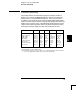
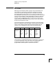
U501. The system memory map is shown below.
Program
ROM U502 contains four 64k x 8 banks of data. Banks are
selected by controlling the
A16 and A17 ROM address bits directly from
CPU port bits.
Custom gate array
U501 performs address latching and memory map
decoding functions as discussed above. In addition,
U501 contains a
variety of internal read/write registers. The read (
XRD) and write (XWR)
signals transfer data out of and in to
U501 when it is addressed. There
are four internal registers in
U501: an internal configuration register,
an 8 bit counter register, a serial transmit/receive register, and an
internal status register.
0000
H
– 1FF7
H
1FF8
H
– 1FFF
H
2000
H
– FFFF
H
U503 8k x 8 RAM
U501 Gate Array
U502 Program ROM
5
Chapter 5 Theory of Operation
Floating Logic
103