Service Guide Publication number 01664-97005 Second edition, January 2000 For Safety information, Warranties, and Regulatory information, see the pages at the end of the book. Copyright Agilent Technologies 1987–2000 All Rights Reserved.
Agilent Technologies 1664A Logic Analyzer The Agilent Technologies 1664A is a 50-MHz State/500-MHz Timing Logic Analyzer. Features Some of the main features of the 1664A Logic Analyzer is as follows: • 32 data channels and 2 clock/data channels • 3.
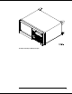
The Agilent Technologies 1664A Logic Analyzer iii
In This Book This book is the service guide for the 1664A Logic Analyzers and is divided into eight chapters. Chapter 1 contains information about the logic analyzer and includes accessories, specifications and characteristics, and equipment required for servicing. Chapter 2 tells how to prepare the logic analyzer for use. Chapter 3 gives instructions on how to test the performance of the logic analyzer. Chapter 4 contains calibration instructions for the logic analyzer.
Table of Contents 1 General Information Accessories 1–2 Specifications 1–3 Characteristics 1–3 Supplemental Characteristics 1–4 Recommended Test Equipment 1–8 2 Preparing for Use To inspect the logic analyzer 2–2 Ferrites 2–3 To apply power 2–4 To operate the user interface 2–4 To set the line voltage 2–4 To degauss the display 2–5 To clean the logic analyzer 2–5 To test the logic analyzer 2–5 3 Testing Performance To perform the self-tests 3–3 To make the test connectors 3–6 To test the threshold accu
Contents To test the multiple-clock, multiple-edge, state acquisition 1–34 Set up the equipment 1–34 Set up the logic analyzer 1–35 Connect the logic analyzer 1–37 Verify the test signal 1–38 Check the setup/hold with single clock edges, multiple clocks 1–40 To test the single-clock, multiple-edge, state acquisition Set up the equipment 1–45 Set up the logic analyzer 1–46 Connect the logic analyzer 1–48 Verify the test signal 1–49 Check the setup/hold combination 1–51 To test the time interval accuracy 1
Contents To remove and replace the Main Circuit board 6–7 To remove and replace the switch actuator assembly 6–8 To remove and replace the rear panel assembly 6–9 To remove and replace the front panel and keyboard 6–10 To remove and replace the intensity adjustment 6–10 To remove and replace the monitor 6–11 To remove and replace the handle plate 6–11 To remove and replace the fan 6–12 To remove and replace the line filter 6–12 To remove and replace the optional GPIB and RS-232C cables 6–13 To return assem
Contents viii
1 Accessories 1-2 Specifications 1-3 Characteristics 1-3 Supplemental Characteristics 1-4 Recommended Test Equipment 1-8 General Information
General Information This chapter lists the accessories, the specifications and characteristics, and the recommended test equipment. Accessories The following accessories are supplied with the 1664A Logic Analyzers.
General Information Specifications Specifications The specifications are the performance standards against which the product is tested. Maximum State Speed 50 MHz * 3.5 ns Minimum State Clock Pulse Width * Minimum Master to Master Clock Time 20.0 ns Minimum Glitch Width* 3.5 ns Threshold Accuracy Setup/Hold Time:* Single Clock, Single Edge Single Clock, Multiple Edges Multiple Clocks, Multiple Edges ± (100 mV + 3% of threshold setting) 0.0/3.5 ns through 3.5/0.0 ns, adjustable in 500-ps increments 0.0/4.
General Information Supplemental Characteristics Supplemental Characteristics Probes Input Resistance Input Capacitance Minimum Voltage Swing 100 kΩ, ± 2% ~ 8 pF 500 mV, peak-to-peak Threshold Range ± 6.0 V, adjustable in 50-mV increments State Analysis State/Clock Qualifiers Time Tag Resolution* Maximum Time Count Between States 6 8 ns or 0.1%, whichever is greater 34 seconds Maximum State Tag Count 4.29 x 10⁹ * Timing Analysis Sample Period Accuracy 0.
General Information Supplemental Characteristics Measurement and Display Functions Displayed Waveforms 24 lines maximum, with scrolling across 96 waveforms. Measurement Functions Run/Stop Functions Run starts acquisition of data in specified trace mode. Stop In single trace mode or the first run of a repetitive acquisition, Stop halts acquisition and displays the current acquisition data. For subsequent runs in repetitive mode, Stop halts acquisition of data and does not change the current display.
General Information Supplemental Characteristics Marker Functions Time Interval The X and O markers measure the time interval between a point on a timing waveform and the trigger, two points on the same timing waveform, two points on different waveforms, or two states (time tagging on). Delta States (state analyzer only) The X and O markers measure the number of tagged states between one state and trigger or between two states.
General Information Supplemental Characteristics Product Regulations Safety EMC Emissions Immunity IEC 348 UL 1244 CSA Standard C22.2 No.231 (Series M-89) This product meets the requirement of the European Communities (EC) EMC Directive 89/336/EEC. EN55011/CSIPR 11 (ISM, Group1,Class A equipment) SABS RAA Act No. 24(1990) EN50082-1 Code1 Notes2 IEC 801-2 (ESD)4kV CD, 8kV AD 2 IEC 801-3 (Rad.) 3V/m 1 2 IEC 801-4 (EFT) 1kV 1 Performance Codes: 1 PASS - Normal operations, no effect.
General Information Recommended Test Equipment Recommended Test Equipment Equipment Required Equipment Critical Specifications Pulse Generator 100 MHz, 3.5 ns pulse width, < 600 ps rise time ≥ 6 GHz bandwidth, < 58 ps rise time Accuracy ≤ (5)(10−6) × frequency, DC offset voltage ±6.3 V 0.1 mV resolution, 0.
2 To inspect the logic analyzer 2-2 Ferrites 2-3 To apply power 2-4 To operate the user interface 2-4 To set the line voltage 2-4 To degauss the display 2-5 To clean the logic analyzer 2-5 To test the logic analyzer 2-5 Preparing for Use
Preparing For Use This chapter gives you instructions for preparing the logic analyzer for use. Power Requirements The logic analyzer requires a power source of either 115 Vac or 230 Vac, –22 % to +10 %, single phase, 48 to 66 Hz, 200 Watts maximum power. Operating Environment The operating environment is listed in chapter 1. Note the noncondensing humidity limitation. Condensation within the instrument can cause poor operation or malfunction. Provide protection against internal condensation.
Preparing for Use Ferrites Ferrites Ferrites are included in the 1664A accessory pouch for the logic analyzer cable. When properly installed, the ferrites reduce RFI emissions from the logic analyzer. In order to ensure compliance of the 1664A Logic Analyzer to the CISPR11 Class A radio frequency interference (RFI) limits, you must install the ferrite to absorb radio frequency energy. Note: Adding or removing the ferrite will not affect the normal operation of the analyzer.
Preparing for Use To apply power To apply power CAUTION Electrostatic discharge can damage electronic components. Use grounded wriststraps and mats when performing any service to the logic analyzer. 1 Check that the line voltage selector, located on the rear panel, is on the correct setting and the correct fuse is installed. See also, "To set the line voltage" on this page. 2 Connect the power cord to the instrument and to the power source. This instrument is equipped with a three-wire power cable.
Preparing for Use To degauss the display 1 Turn the power switch to the Off position, then remove the power cord from the instrument. 2 Remove the fuse module by carefully prying at the top center of the fuse module until you can grasp it and pull it out by hand. 3 Reinsert the fuse module with the arrow for the appropriate line voltage aligned with the arrow on the line filter assembly switch. 4 Reconnect the power cord. Turn on the instrument by setting the power switch to the On position.
2–6
3 To perform the self-tests 3-3 To make the test connectors 3-6 To test the threshold accuracy 3-8 To test the glitch capture 3-17 To test the single-clock, single-edge, state acquisition 3-23 To test the multiple-clock, multiple-edge, state acquisition 3-34 To test the single-clock, multiple-edge, state acquisition 3-45 To test the time interval accuracy 3-54 Performance Test Record 3-59 Testing Performance
Testing Performance This chapter tells you how to test the performance of the logic analyzer against the specifications listed in chapter 1. To ensure the logic analyzer is operating as specified, you perform software tests (self-tests) and manual performance tests on the analyzer. The logic analyzer is considered performance-verified if all of the software tests and manual performance tests have passed. The procedures in this chapter indicate what constitutes a "Pass" status for each of the tests.
To perform the self-tests The self-tests verify the correct operation of the logic analyzer. Self-tests can be performed all at once or one at a time. While testing the performance of the logic analyzer, run the self-tests all at once. 1 Disconnect all inputs, insert the boot disk, then turn on the power switch. Wait until the power-up tests are complete. 2 Press the System key. Select the field next to System, then select Test in the pop-up menu then press the Select key.
Testing Performance To perform the self-tests 7 Select the Printer/Controller field next to Sys PV, then select System Test in the pop-up menu then press the Select key. 8 Install a formatted disk that is not write protected into the disk drive. If the 1664A has the RS-232C option (020), connect an RS-232C loopback connector onto the RS-232C port. 9 Select All System Tests. You can run all tests at one time, except for the Front Panel Test and Display Test, by running All System Tests.
Testing Performance To perform the self-tests 11 Select the Display Test. A white grid pattern is displayed. These display screens are not normally used, but can be used to adjust the display. Refer to chapter 4, "Calibrating and Adjusting" for display adjustments. a Select Continue and the screen changes to full bright. b Select Continue and the screen changes to half bright. c Select Continue and the test screen shows the Display Test status changed to Tested.
To make the test connectors The test connectors connect the logic analyzer to the test equipment. Materials Required Description Recommended Part Qty BNC (f) Connector Agilent 1250-1032 5 100 Ω 1% resistor Agilent 0698-7212 8 Berg Strip, 17-by-2 1 Berg Strip, 6-by-2 4 20:1 Probe Agilent 54006A 2 Jumper wire 1 Build four test connectors using BNC connectors and 6-by-2 sections of Berg strip. a Solder a jumper wire to all pins on one side of the Berg strip.
Testing Performance To make the test connectors 2 Build one test connector using a BNC connector and a 17-by-2 section of Berg strip. a Solder a jumper wire to all pins on one side of the Berg strip. b Solder a jumper wire to all pins on the other side of the Berg strip. c Solder the center of the BNC connector to the center pin of one row on the Berg strip. d Solder the ground tab of the BNC connector to the center pin of the other row on the Berg strip.
To test the threshold accuracy Testing the threshold accuracy verifies the performance of the following specification: • Clock and data channel threshold accuracy. These instructions include detailed steps for testing the threshold settings of pod 1. After testing pod 1, connect and test pod 2. To test pod 2, follow the detailed steps for pod 1, substituting the pod 2 for pod 1 in the instructions.
Testing Performance To test the threshold accuracy Set up the logic analyzer 1 Press the Config key. Assign all pod fields to Machine 1. To assign the pod fields, select the pod fields, then select Machine 1 in the pop-up menu. 2 In the Analyzer 1 box, select the Type field. Select Timing in the pop-up menu. Connect the logic analyzer 1 Using the 17-by-2 test connector, BNC cable, and probe tip assembly, connect the data and clock channels of pod 1 to one side of the BNC Tee.
Testing Performance To test the threshold accuracy Test the TTL threshold 1 Press the Format key. Select the field to the right of Pod 1, then select TTL in the pop-up menu. 2 On the function generator front panel, enter 1.647 V ±1 mV DC offset. Use the multimeter to verify the voltage. The activity indicators for pod 1 should show all data channels and the J-clock channel at a logic high.
Testing Performance To test the threshold accuracy 4 Using the Modify up arrow on the function generator, increase offset voltage in 1-mV increments until all activity indicators for pod 1 show the channels at a logic high. Record the function generator voltage in the performance test record.
Testing Performance To test the threshold accuracy Test the ECL threshold 1 Select the field to the right of Pod 1, then select ECL in the pop-up menu. 2 On the function generator front panel, enter −1.160 V ±1 mV DC offset. Use the multimeter to verify the voltage. The activity indicators for pod 1 should show all data channels and the J-clock channel at a logic high.
Testing Performance To test the threshold accuracy Test the − User threshold 1 Move the cursor to the field to the right of Pod 1. Type –6.00, then use the left and right cursor control keys to highlight V. Press the Select key. 2 On the function generator front panel, enter −5.718 V ±1 mV DC offset. Use the multimeter to verify the voltage. The activity indicators for pod 1 should show all data channels and the J-clock channel at a logic high.
Testing Performance To test the threshold accuracy Test the + User threshold 1 Move the cursor to the field to the right of Pod 1. Type +6.00, then use the left and right cursor control keys to highlight V. Press the Select key. 2 On the function generator front panel, enter +6.282 V ±1 mV DC offset. Use the multimeter to verify the voltage. The activity indicators for pod 1 should show all data channels and the J-clock channel at a logic high.
Testing Performance To test the threshold accuracy Test the 0 V User threshold 1 Move the cursor to the field to the right of Pod 1. Type 0, then press the Select key. 2 On the function generator front panel, enter +0.102 V ±1 mV DC offset. Use the multimeter to verify the voltage. The activity indicators for pod 1 should show all data channels and the J-clock channel at a logic high.
Testing Performance To test the threshold accuracy Test the next pod 1 Using the 17-by-2 test connector and probe tip assembly, connect the data and clock channels of pod 2 to the output of the function generator. 2 Start with "Test the TTL threshold" on page 3−10, substituting pod 2 for pod 1.
To test the glitch capture Testing the glitch capture verifies the performance of the following specification: • Minimum detectable glitch. This test checks the minimum detectable glitch on sixteen data channels at a time. Equipment Required Equipment Pulse Generator Digitizing Oscilloscope SMA Coax (Qty 3) Adapter (Qty 4) Coupler (Qty 4) BNC Test Connector, 6x2 (Qty 4) Critical Specifications 100 MHz 3.
Testing Performance To test the glitch capture 3 Set up the oscilloscope. Oscilloscope Setup Time Base Display Delta V Delta T Time/Div: 1.00 ns/div mode: avg V markers on T markers on delay: 17.7000 ns # of avg: 16 marker 1 position: Chan 1 start on: Pos Edge 1 screens: dual marker 2 position: Chan 2 stop on: Pos Edge 1 Channel 1 Channel 2 Display on on Probe Atten 20.00 20.00 Volts/Div 400 mV 400 mV Offset −1.3000 V −1.
Testing Performance To test the glitch capture Connect the Logic Analyzer to the Pulse Generator Testing Combinations To Agilent 8131A Channel 1 Output To 8131A Channel 1 Output To 8131A Channel 2 Output To 8131A Channel 2 Output 1 Pod 1 ch 0, 2, 4, 6, J-clock Pod 1 ch 1, 3, 5, 7 Pod 1 ch 8, 10, 12, 14 Pod 1 ch 9, 11, 13, 15 2 Pod 2 ch 0, 2, 4, 6, K-clock Pod 2 ch 1, 3, 5, 7 Pod 2 ch 8, 10, 12, 14 Pod 2 ch 9, 11, 13, 15 3–19
Testing Performance To test the glitch capture Test the glitch capture on the connected channels 1 Set up the Format menu. a Press the Format key. b Select the field to the right of the pod, then select ECL in the pop-up menu. Use the arrow keys to access pods not shown on the screen (select the Pods field and push Select). c Select Timing Acquisition Mode, then select Glitch Half Channel 125 MHz. 2 Turn on the channels that correspond to the channels being tested.
Testing Performance To test the glitch capture 3 Set up the Trigger menu. a Press the Trigger key. b Select Modify Trigger, then Clear Trigger, then select All in the pop-up menus. 4 Using the Precision Edge Find in the Delta T menu of the oscilloscope, verify that the pulse widths of the pulse generator channels 1 and 2 are 3.450 ns, +50 ps or −100 ps. If necessary, adjust the pulse widths of the pulse generator channels 1 and 2. 5 Set up the Waveform menu to view all the channels.
Testing Performance To test the glitch capture 6 On the logic analyzer, press the Run key. The display should be similar to the figure below. 7 On the pulse generator, enable Channel 1 and Channel 2 COMP (with the LED on). 8 On the logic analyzer, press the Run key. The display should be similar to the figure below. Record Pass or Fail in the performance test record.
To test the single-clock, single-edge, state acquisition Testing the single-clock, single-edge, state acquisition verifies the performance of the following specifications: • • • • Minimum master to master clock time. Maximum state acquisition speed. Setup/Hold time for single-clock, single-edge, state acquisition. Minimum clock pulse width. This test checks the data channels using a single-edge clock at three selected setup/hold times.
Testing Performance To test the single-clock, single-edge, state acquisition 3 Set up the oscilloscope. Oscilloscope Setup Time Base Display Delta V Delta T Time/Div: 1.00 ns/div avg V markers on T markers on # of avg: 16 marker 1 position: Chan 1 start on: Pos Edge 1 screen: dual marker 2 position: Chan 1 stop on: Neg Edge 1 Channel Channel 1 Channel 2 Display on on Probe Atten 20.00 20.00 Offset −1.3 V −1.
Testing Performance To test the single-clock, single-edge, state acquisition 2 Set up the Format menu. a Press the Format key. Select State Acquisition Mode, then select Full Channel/4K Memory/50MHz. b Select the field to the right of each pod, then select ECL in the pop-up menu. 3 Set up the Trigger menu. a Press the Trigger key. Select Modify Trigger, then Clear Trigger, then select All in the pop-up menus. b Select Count Off. Press Select again, then select Time in the pop-up menu.
Testing Performance To test the single-clock, single-edge, state acquisition Connect the logic analyzer 1 Using the 6-by-2 test connectors, connect the logic analyzer clock and data channels listed in the following table to the pulse generator. Install a BNC cable between the pulse generator channel 2 output and the 6x2 test connector with the logic analyzer clock leads. 2 Using SMA cables, connect the oscilloscope to the pulse generator channel 1 Output, channel 2 Output, and Trig Output.
Testing Performance To test the single-clock, single-edge, state acquisition c Press the Trigger key. Make sure pattern term a is "A". If not, select the field next to "a" under the label Lab1. Type "A", then press the Select key. Verify the test signal 1 Check the clock pulse width. Using the oscilloscope, verify that the clock pulse width is 3.50 ns, +0 ps or −100 ps. a Enable the pulse generator channel 1 and channel 2 outputs. b In the oscilloscope Timebase menu, select Delay.
Testing Performance To test the single-clock, single-edge, state acquisition c In the oscilloscope Measure menu, select Measure Chan 2, then select Period. If the period is more than or equal to 20.000 ns, go to step 4. If the period is less than 20.000 ns but greater than 19.75 ns, go to step 3. d In the oscilloscope Timebase menu, add 10 ns to the delay. e In the oscilloscope Measure menu, select Period. If the period is more than or equal to 20.
Testing Performance To test the single-clock, single-edge, state acquisition Check the setup/hold combination 1 Select the logic analyzer setup/hold time. a In the logic analyzer Format menu, select Master Clock. b Select the Setup/Hold field, then select the setup/hold combination to be tested for all pods. The first time through this test, use the top combination in the following table. Setup/Hold Combinations 3.5/0.0 ns 0.0/3.5 ns 1.5/2.0 ns c Select Done to exit the setup/hold combinations.
Testing Performance To test the single-clock, single-edge, state acquisition c Adjust the pulse generator channel 1 Delay, then select Precision Edge Find in the oscilloscope Delta T menu. Repeat this step until the pulses are aligned according to the setup time of the setup/hold combination selected, +0.0 ps or −100 ps. 4 Select the clock to be tested. a In the Master Clock menu, select the clock field to be tested, then select the clock edge as indicated in the table.
Testing Performance To test the single-clock, single-edge, state acquisition 5 Note: This step is only done the first time through the test, to create a Compare file. For subsequent runs, go to step 6. Use the following to create a Compare file: a Press Run. The display should show a checkerboard pattern of alternating As and 5s. Verify the pattern by scrolling through the display. b Press the List key. In the pop up menu, use the RPG knob to move the cursor to Compare. Press Select.
Testing Performance To test the single-clock, single-edge, state acquisition 10 Using the Delay mode of the pulse generator channel 1, position the pulses according to the setup/hold combination selected, +0.0 ps or −100 ps. a In the oscilloscope Delta V menu, set the Marker 1 Position to Chan 1, then set Marker 1 at −1.3000 V. Set the Marker 2 Position to Chan 2, then set Marker 2 at −1.3000 V. b In the oscilloscope Delta T menu, select Start on Pos Edge 1. Select Stop on Neg Edge 1.
Testing Performance 12 Press the blue shift key, then press the Run key. If 2 - 4 acquisitions are obtained without the "Stop Condition Satisfied" message appearing, then the test passes. Press Stop to halt the acquisition. Record the Pass or Fail results in the performance test record. 13 Test the next clock. a Press the Format key, then select Master Clock. b Turn off and disconnect the clock just tested.
To test the multiple-clock, multiple-edge, state acquisition Testing the multiple-clock, multiple-edge, state acquisition verifies the performance of the following specifications: • • • • Minimum master to master clock time. Maximum state acquisition speed. Setup/Hold time for multiple-clock, multiple-edge, state acquisition. Minimum clock pulse width. This test checks data using multiple clocks at three selected setup/hold times.
Testing Performance To test the multiple-clock, multiple-edge, state acquisition 3 Set up the oscilloscope. Oscilloscope Setup Time Base Display Delta V Delta T Time/Div: 1.00 ns/div avg V markers on T markers on # of avg: 16 marker 1 position: Chan 1 start on: Pos Edge 1 screen: dual marker 2 position: Chan 1 stop on: Neg Edge 1 Channel Channel 1 Channel 2 Display on on Probe Atten 20.00 20.00 Offset −1.3 V −1.
Testing Performance To test the multiple-clock, multiple-edge, state acquisition 2 Set up the Format menu. a Press the Format key. Select State Acquisition Mode, then select Full Channel/4K Memory/50MHz. b Select the field to the right of each Pod field, then select ECL. 3 Set up the Trigger menu. a Press the Trigger key. Select Clear Trigger, then select All. b Select the Count Off field, then select Time in the pop-up menu. Select Done to exit the menu.
Testing Performance To test the multiple-clock, multiple-edge, state acquisition Connect the logic analyzer 1 Using the 6-by-2 test connectors, connect the logic analyzer clock and data channels listed in the following table to the pulse generator. Install a BNC cable between the pulse generator channel 2 output and the 6x2 test connector with the logic analyzer clock leads. 2 Using SMA cables, connect channel 1, channel 2, and trigger of the oscilloscope to the pulse generator.
Testing Performance To test the multiple-clock, multiple-edge, state acquisition c Press the Trigger key. Make sure pattern term a is "A". If not, select the field next to "a" under the label Lab1. Type "A" then press the Select key. Verify the test signal 1 Check the clock pulse width. Using the oscilloscope, verify that the clock pulse width is 3.50 ns, +0 ps or −100 ps. a Enable the pulse generator channel 1 and channel 2 outputs (with the LED off). b In the oscilloscope Timebase menu, select Delay.
Testing Performance To test the multiple-clock, multiple-edge, state acquisition c In the oscilloscope Measure menu, select Measure Chan 2, then select Period. If the period is more than or equal to 20.000 ns, go to step 4. If the period is less than 20.000 ns but greater than 19.75 ns, go to step 3. d In the oscilloscope Timebase menu, add 10 ns to the Delay. e In the oscilloscope Measure menu, select Period. If the period is more than or equal to 20.
Testing Performance To test the multiple-clock, multiple-edge, state acquisition Check the setup/hold with single clock edges, multiple clocks 1 Select the logic analyzer setup/hold time. a In the logic analyzer Format menu, select Master Clock. b Select and activate any two clock edges. c Select the Setup/Hold field and select the setup/hold to be tested for all pods. The first time through this test, use the top combination in the following table. Setup/Hold Combinations 4.5/0.0 ns 0.0/4.5 ns 2.0/2.
Testing Performance To test the multiple-clock, multiple-edge, state acquisition c Adjust the pulse generator channel 1 Delay, then select Precision Edge Find in the oscilloscope Delta T menu. Repeat this step until the pulses are aligned according to the setup time of the setup/hold combination selected, +0.0 ps or −100 ps. 4 Select the clocks to be tested. a Select the clock field to be tested and then select J↑ + K↑ as the clock edges. b Select Done to exit the Master Clock menu.
Testing Performance To test the multiple-clock, multiple-edge, state acquisition 5 If you have not already created a Compare file for the previous test (single-clock, single-edge state acquisition, page 3-31), use the following steps to create one. For subsequent passes through this test, skip this step and go to step 6. a Press Run. The display should show a checkerboard pattern of alternating As and 5s. Verify the pattern by scrolling through the display. b Press the List key.
Testing Performance To test the multiple-clock, multiple-edge, state acquisition 9 Using the Delay mode of the pulse generator channel 1, position the pulses according to the setup time of the setup/hold combination selected, +0.0 ps or −100 ps. a In the oscilloscope Delta V menu, set the Marker 1 Position to Chan 1, then set Marker 1 at −1.3000 V. Set the Marker 2 Position to Chan 2, then set Marker 2 at −1.3000 V. b In the oscilloscope Delta T menu, select Start On Pos Edge 1. Select Stop on Neg Edge 1.
Testing Performance To test the multiple-clock, multiple-edge, state acquisition 11 Press the blue shift key, then press the Run key. If 2 - 4 acquisitions are obtained without the "Stop Condition Satisfied" message appearing, then the test passes. Press Stop to halt the acquisition. Record the Pass or Fail results in the performance test record. 12 Test the next setup/hold combination. a In the logic analyzer Format menu, select Master Clock. b Turn off and disconnect the clocks just tested.
To test the single-clock, multiple-edge, state acquisition Testing the single-clock, multiple-edge, state acquisition verifies the performance of the following specifications: • Minimum master to master clock time. • Maximum state acquisition speed. • Setup/Hold time for single-clock, multiple-edge, state acquisition. This test checks data channels using a multiple-edge single clock at three selected setup/hold times.
Testing Performance To test the single-clock, multiple-edge, state acquisition 3 Set up the oscilloscope. Oscilloscope Setup Time Base Display Delta V Delta T Time/Div: 1.00 ns/div avg V markers on T markers on # of avg: 16 marker 1 position: Chan 1 start on: Neg Edge 1 screen: dual marker 2 position: Chan 1 stop on: Neg Edge 2 Channel Channel 1 Channel 2 Display on on Probe Atten 20.00 20.00 Offset −1.3 V −1.
Testing Performance To test the single-clock, multiple-edge, state acquisition 2 Set up the Format menu. a Press the Format key. Select State Acquisition Mode, then select Full Channel/4K Memory/50MHz. b Select the field to the right of each pod field, then select ECL. 3 Set up the Trigger menu. a Press the Trigger key. Select Clear Trigger, then select All. b Select the Count Off field, then select Time in the pop-up menu. Select Done to exit the menu.
Testing Performance To test the single-clock, multiple-edge, state acquisition Connect the logic analyzer 1 Using the 6-by-2 test connectors, connect the logic analyzer clock and data channels listed in the following table to the pulse generator. Install a BNC cable between the pulse generator channel 2 output and the 6x2 test connector with the logic analyzer clock leads. 2 Using SMA cables, connect channel 1, channel 2, and trigger of the oscilloscope to the pulse generator.
Testing Performance To test the single-clock, multiple-edge, state acquisition c Press the Trigger key. Make sure pattern term a is "A". If not, select the field next to "a" under the label Lab1. Type "A" then press the Select key. Verify the test signal 1 Check the clock period. Using the oscilloscope, verify that the clock period is 20 ns, +0 ps or −250 ps. a In the oscilloscope Timebase menu, select Sweep Speed 4.00 ns/div. b Select Delay.
Testing Performance To test the single-clock, multiple-edge, state acquisition 2 Check the data pulse width. Using the oscilloscope, verify that the data pulse width is 4.000 ns, +0 ps or −100 ps. a In the oscilloscope Timebase menu, select Sweep Speed 1.00 ns/div. b Select Delay. Using the oscilloscope knob, position the data waveform (Channel 1) so that the waveform is centered on the screen. c In the oscilloscope Delta V menu, set the Marker 1 Position to Chan 1, then set Marker 1 at −1.3000 V.
Testing Performance To test the single-clock, multiple-edge, state acquisition Check the setup/hold combination 1 Select the logic analyzer setup/hold time. a In the logic analyzer Format menu, select Master Clock. NOTE The first time through this test, assign the clocks according to the first testing combination in step 3 of these procedures. b In the Master Clock menu, select Setup/Hold.
Testing Performance To test the single-clock, multiple-edge, state acquisition c Adjust the pulse generator channel 2 Delay, then select Precision Edge Find in the oscilloscope Delta T menu. Repeat this step until the pulses are aligned according to the setup time of the setup/hold combination selected, +0.0 ps or −100 ps. NOTE If the rising clock edge does not appear on the oscilloscope display, then add 20.0 ns to the oscilloscope Timebase Delay. 3 Select the clock to be tested.
Testing Performance To test the single-clock, multiple-edge, state acquisition 6 Test the next clock. a Press the Format key, then select Master Clock. b Turn off and disconnect the clock just tested. c Repeat steps 3 and 5 for the next clock listed in the table in step 3, until all listed clock edges have been tested. 7 Test the next setup/hold combination. a Press the Format key, then select Master Clock and turn off the clock just tested.
To test the time interval accuracy Testing the time interval accuracy does not check a specification, but does check the following: • 125 MHz oscillator This test verifies that the 125 MHz timing acquisition synchronizing oscillator is operating within limits. Equipment Required Equipment Critical Specifications Recommended Model/Part Pulse Generator 100 MHz 3.
Testing Performance To test the time interval accuracy 3 Set up the function generator according to the following table. Function Generator Setup Freq: 200 000 . 0 Hz Main Function: Square wave Amptd: 3.000 V High Voltage: Disabled (LED Off) Phase: 0.0 deg DC Offset: 0.0 V Set up the logic analyzer 1 Set up the Configuration menu. a Press the Config key. b In the Configuration menu, assign Pod 1 to Machine 1. To assign Pod 1, select the Pod 1 field, then select Machine 1.
Testing Performance To test the time interval accuracy 2 Set up the Format menu. a Press the Format key. Select Timing Acquisition Mode, then select Transitional Full Channel 125 MHz. b Select the field to the right of the Pod 1 field, then select ECL. c Select the field showing the channel assignments for Pod 1. Deactivate all channels by pressing the Clear entry key. Using the arrow keys, move the selector to Channel 0.
Testing Performance To test the time interval accuracy 4 Set up the Waveform menu. a Press the Waveform key. b Move the cursor to the sec/Div field, then use the RPG knob to dial in 2.00 µs. c Select the Markers Off field, then select Pattern. d Select the Specify Patterns field. Select X entering 1 and O entering 1. e f g h Select Done to exit the Specify Patterns menu. Move the cursor to the X-pat field. Type 1, then press Done. Move the cursor to the O-pat field. Type 20, then press Done.
Testing Performance To test the time interval accuracy Acquire the data 1 Enable the pulse generator channel 1 output (with the LED off). 2 Press the blue key, then press the Run key to select Run-Repetitive. Allow the logic analyzer to acquire data for at least 100 valid runs as indicated in the pattern statistics field. 3 When the logic analyzer has acquired at least 100 valid runs, touch Stop. The Min X-O field in the logic analyzer Pattern Statistics menu should read 94.99–95.00 µs.
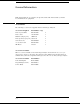
Performance Test Record Performance Test Record 1664A Logic Analyzer_______ Serial No.______________________ Work Order No.___________________ Recommended Test Interval - 2 Year/4000 hours Date___________________ Recommended next testing___________________ Temperature___________________ Test Settings Results Pass/Fail ________ Limits Measured TTL VL TTL VH ECL VL ECL VH -User VL - User VH + User VL + User VH 0 V User VL 0 V User VH +1.355 V +1.645 V -1.439 V -1.161 V -6.280 V -5.720 V +5.
Performance Test Record (continued) Test Settings Results Pass/Fail Single-Clock, Single-Edge Acquisition Pass/Fail Setup/Hold Time 3.5/0.0 ns J↑ K↑ ________ ________ J↓ K↓ ________ ________ Setup/Hold Time 0.0/3.5 ns J↑ K↑ ________ ________ J↓ K↓ ________ ________ Setup/Hold Time 1.5/2.5 ns J↑ K↑ ________ ________ J↓ K↓ ________ ________ Multiple-Clock, Multiple-Edge Acquisition Pass/Fail Pass/Fail Setup/Hold Time 4.5/0.
4 Logic analyzer calibration 4-2 To adjust the CRT monitor alignment 4-3 To adjust the CRT intensity 4-5 Calibrating and Adjusting
Calibrating and Adjusting This chapter gives you instructions for calibrating and adjusting the logic analyzer. Adjustments to the logic analyzer include adjusting the CRT monitor assembly. To periodically verify the performance of the analyzer, refer to "Testing Performance" in chapter 3. Logic analyzer calibration The logic analyzer circuitry of the 1664A Logic Analyzer does not require an operational accuracy calibration.
To adjust the CRT monitor alignment WARNING Do not touch the CRT monitor sweep board. High voltages exist on the sweep board that can cause personal injury. Equipment Required Equipment Critical Specification Recommended Model/Part Alignment Tool 1 8710-1300 1 Turn off the logic analyzer, then disconnect the power cord. Remove the cover. Refer to chapter 6, "Replacing Assemblies," for instructions to remove the cover.
Calibrating and Adjusting To adjust the CRT monitor alignment 4 Enter the Sys PV tests, then enter the Display Test. A grid pattern should appear. 5 If the display is tilted (rotated), adjust the CRT yoke by rotating it to straighten the display. Yoke 6 If the grid pattern is not centered horizontally, adjust the H-Hold. 7 If you need to adjust the intensity, go to the next page. If you are finished with the adjustments, turn off the instrument, then remove the power cord.
To adjust the CRT intensity WARNING Do not touch the CRT monitor sweep board. High voltages exist on the sweep board that can cause personal injury. Equipment Required Equipment Critical Specification Recommended Model/Part Alignment Tool 1 8710-1300 Light Power Meter United Detector 351 1 Turn off the logic analyzer, then disconnect the power cord. Remove the cover. Refer to chapter 6, "Replacing Assemblies," for instructions to remove the cover.
Calibrating and Adjusting To adjust the CRT intensity WARNING Do not touch the CRT monitor sweep board. High voltages exist on the sweep board that can cause personal injury. 2 7 The light power meter should read 137-154 cd/m . If the measurement is out of this range, use the adjustment tool to adjust the Contrast potentiometer on the monitor driver board. 8 Press the front panel Select key. The display should show a half bright test screen.
5 To use the flowcharts 5-2 To check the power-up tests 5-15 To run the self-tests 5-16 To test the power supply voltages 5-21 To test the CRT monitor signals 5-23 To test the keyboard signals 5-24 To test the disk drive voltages 5-25 To perform the BNC test 5-27 To test the logic analyzer probe cables 5-28 To test the auxiliary power 5-32 Troubleshooting
Troubleshooting This chapter helps you troubleshoot the logic analyzer to find defective assemblies. The troubleshooting consists of flowcharts, self-test instructions, and tests. This information is not intended for component-level repair. If you suspect a problem, start at the top of the first flowchart. During the troubleshooting instructions, the flowcharts will direct you to perform other tests. The service strategy for this instrument is the replacement of defective assemblies.
Troubleshooting To use the flowcharts Troubleshooting Flowchart 1 5–3
Troubleshooting To use the flowcharts Troubleshooting Flowchart 2 5–4
Troubleshooting To use the flowcharts Troubleshooting Flowchart 3 5–5
Troubleshooting To use the flowcharts Troubleshooting Flowchart 4 5–6
Troubleshooting To use the flowcharts Troubleshooting Flowchart 5 5–7
Troubleshooting To use the flowcharts Troubleshooting Flowchart 6 5–8
Troubleshooting To use the flowcharts Troubleshooting Flowchart 7 5–9
Troubleshooting To use the flowcharts Troubleshooting Flowchart 8 5–10
Troubleshooting To use the flowcharts Troubleshooting Flowchart 9 5–11
Troubleshooting To use the flowcharts Troubleshooting Flowchart 10 5–12
Troubleshooting To use the flowcharts Troubleshooting Flowchart 11 5–13
Troubleshooting To use the flowcharts Troubleshooting Flowchart 12 5–14
Troubleshooting To check the power-up tests To check the power-up tests The logic analyzer automatically performs power-up tests when you apply power to the instrument (during the boot-up sequence). The revision number of the operating system shows in the upper-right corner of the screen during these power-up tests. As each test completes, either "passed" or "failed" prints on the screen in front of the name of each test. 1 Disconnect all inputs, then insert the operating system disk into the disk drive.
Troubleshooting To run the self-tests To run the self-tests Self-tests identify the correct operation of major functional areas of the instrument. You can run all self-tests without accessing the interior of the instrument. If a self-test fails, the troubleshooting flowcharts instruct you to change a part of the instrument. 1 If you just did the power-up self-tests, go to step 2.
Troubleshooting To run the self-tests 6 Select Run, then select Single. The test runs one time, then the screen shows the results. When the test is finished, select Done. To run a test continuously, select Repetitive. Select Stop to halt a Run Repetitive. 7 Select Board Tests, then select Run. When the Board Tests are finished, select Done. 8 Select Data Input Inspection. All lines should show activity. Select Done to exit the Data Input Inspection.
Troubleshooting To run the self-tests 10 Select the Printer/Controller field next to Sys PV. Select System Test and press the Select key to access the system tests. You can run all tests at one time by running All System Tests. To see more details about each test, you can run each test individually. This example shows how to run an individual test. 11 Select ROM Test. The ROM Test screen is displayed. 12 Select Run, then select Single. To run a test continuously, select Repetitive.
Troubleshooting To run the self-tests For a Single run, the test runs one time, and the screen shows the results. 13 To exit the ROM Test, select Done. Note that the status changes to Passed or Failed. 14 Install a formatted disk that is not write protected into the disk drive. If option 020 is installed, connect an RS-232C loopback connector onto the RS-232C port. Run the remaining System Tests in the same manner.
Troubleshooting To run the self-tests 17 To exit the tests, press the System key, then select Exit Test in the pop-up menu and press the select key. Reinstall the disk containing the operating system, then select Exit Test System and press the select key. If you are performing the self-tests as part of the troubleshooting flowchart, return to the flowchart.
Troubleshooting To test the power supply voltages To test the power supply voltages To check the voltages, the power supply must be loaded by either the acquisition board or with an added resistor. Refer to chapter 6, "Replacing Assemblies," for instructions to remove or replace covers and assemblies. WARNING Hazard voltages exist on the power supply, the CRT, and the CRT driver board.
Troubleshooting To test the power supply voltages 6 Check for the voltages on the power supply cable using the values in the following table. Signals on the Power Supply Cable Pin Signal Pin Signal 1 +5.00 V 11 –5.20 V 2 +5.00 V 12 Ground 3 +5.00 V 13 +12 V 4 +5.00 V 14 Ground 5 Ground (Digital) 15 –12 V 6 Ground (Digital) 16 Ground 7 Ground (Digital) 17 +12 V (Display) 8 Ground (Display) 18 –5.20 V 9 +3.
Troubleshooting To test the CRT monitor signals To test the CRT monitor signals Refer to chapter 6, "Replacing Assemblies," for instructions to remove or replace covers and assemblies. WARNING Hazard voltages exist on the power supply, the CRT, and the CRT driver board. This procedure is to be performed by service-trained personnel aware of the hazards involved, such as fire and electrical shock. 1 Remove the cover of the instrument.
Troubleshooting To test the keyboard signals To test the keyboard signals Refer to chapter 6, "Replacing Assemblies," for instructions to remove covers and assemblies. WARNING Hazard voltages exist on the power supply, the CRT, and the CRT driver board. This procedure is to be performed by service-trained personnel aware of the hazards involved, such as fire and electrical shock. 1 Turn off the instrument and remove the power cable.
Troubleshooting To test the disk drive voltages To test the disk drive voltages Refer to chapter 6, "Replacing Assemblies," for instructions to remove or replace covers and assemblies. WARNING This procedure is to be performed by service-trained personnel aware of the hazards involved, such as fire and electrical shock.
Troubleshooting To test the disk drive voltages 6 Check for the following voltages and signals using an oscilloscope.
Troubleshooting To perform the BNC test To perform the BNC test Equipment Required Equipment Critical Specification Recommended Model/Part Digitizing Oscilloscope 100 MHz Bandwidth Agilent 54600A BNC Shorting Cap 1250-0074 BNC Cable Agilent 10503A BNC-Banana Adapter 1251-2277 1 Press the Config key. 2 Assign pods 1 and 2 to Machine 1. To assign the pod field, select the pods 1 and 2 field, then select Machine 1 in the pop-up menu. 3 In the Analyzer 1 box, select the Type field.
Troubleshooting To test the logic analyzer probe cables To test the logic analyzer probe cables This test allows you to functionally verify the probe cable and probe tip assembly of any of the logic analyzer pods. Only one probe cable can be tested at a time. Repeat this test for each probe cable to be tested. Equipment Required Equipment Critical Specification Recommended Model/Part Pulse Generator 100 MHz, 3.
Troubleshooting To test the logic analyzer probe cables 4 Set up the Format menu. a Press the Format key. b Move the cursor to the field showing the channel assignments for the pod under test. Press the Clear Entry key until the pod channels are all assigned (all asterisks (*)). Press the Done key. c Select Master Clock, then select a double edge for the clock of the pod under test. Turn off the other clocks. d In the Master Clock menu, select Setup/Hold, then select 4.0/0.0 ns for the pod being tested.
Troubleshooting To test the logic analyzer probe cables e Select the field to the right of the pod being tested, then select TTL. 5 Set up the Trigger menu. a Press the Trigger key. b Select Clear Trigger, then select All. 6 Set up the Listing menu. a Press the List key. b Select the field to the right of Base, then select Binary.
Troubleshooting To test the logic analyzer probe cables 7 Using four 6-by-2 test connectors, four BNC Couplers, and four SMA (m) - BNC (f) Adapters, connect the logic analyzer to the pulse generator channel outputs. To make the test connectors, see chapter 3, "Testing Performance." a Connect the even-numbered channels of the lower byte of the pod under test to the pulse generator channel 1 Output and J-clock.
Troubleshooting To test the auxiliary power To test the auxiliary power The +5 V auxiliary power is protected by a current overload protection device. If the current on pins 1 and 39 exceed 0.33 amps, the circuit will open. When the short is removed, the circuit will reset in approximately 1 minute. There should be +5 V after the 1 minute reset time. Equipment Required Equipment Critical Specifications Recommended Model/Part Digital Multimeter 0.1 mV resolution, better than Agilent 3478A 0.
6 To remove and replace the Handle 6-5 Feet and tilt stand 6-5 Cover 6-5 Disk drive 6-6 Power supply 6-7 Main circuit board 6-7 Switch actuator assembly 6-8 Rear panel assembly 6-9 Front panel and keyboard 6-10 Intensity adjustment 6-10 Monitor 6-11 Handle plate 6-11 Fan 6-12 Line filter 6-12 Optional GPIB and/or RS-232C cables 6-13 To return assemblies 6-14 Replacing Assemblies
Replacing Assemblies This chapter contains the instructions for removing and replacing the assemblies of the logic analyzer. Also in this chapter are instructions for returning assemblies. WARNING CAUTION Hazardous voltages exist on the power supply, the CRT, and the CRT driver board. To avoid electrical shock, disconnect the power from the instrument before performing the following procedures.
Replacing Assemblies Exploded View Listing A1 A2 A3 A4 A5 Main circuit board Keyboard Switch actuator Probe cable Probe tip MP3 MP4 MP5 MP6 MP7 Fan guard Rear panel Line filter Handle plate Ground bracket MP32 MP33 Spacer Label W1 W2 Fan cable Disk drive cable A6 A7 A8 A9 Power supply Disk drive Monitor assembly Fan H2 H3 Ground spring Locking pin MP8 MP9 MP15 MP18 MP19 MP20 MP21 Cabinet Cover Rear feet Mounting plate Insulator Trim strip Label W3 W4 W5 W6 W7 W8 W9 Jumper cable-orange Jumper
Replacing Assemblies Exploded View of the 1664A 6–4
Replacing Assemblies To remove and replace the handle To remove and replace the handle • Remove the two screws in the endcaps, then lift off the handle. To remove and replace the feet and tilt stand Remove the screws connecting the four rear feet to the instrument. Separate the rear feet from the instrument to remove them. Press the locking tab on the bottom feet, then remove them. Remove the tilt stand from the bottom front feet by lifting the stand up and out of the foot.
Replacing Assemblies To remove and replace the disk drive To remove and replace the disk drive 1 Using previous procedures, remove the following assemblies: • Handle • Rear Feet • Cover 2 3 4 5 Disconnect the disk drive cable from the rear of the disk drive. Remove the two screws that attach the disk drive bracket to the power supply. Slide the disk drive toward the rear of the instrument, then lift it up and out. Remove the disk drive bracket.
Replacing Assemblies To remove and replace the power supply To remove and replace the power supply 1 Using previous procedures, remove the following assemblies: • • • • Handle Rear Feet Cover Disk Drive Hazardous voltages exist on the power supply. To avoid electrical shock, disconnect the power from the instrument before performing the following procedures. After disconnecting the power, wait at least three minutes for the capacitors to discharge before servicing the instrument.
Replacing Assemblies To remove and replace the switch actuator assembly To remove and replace the switch actuator assembly 1 Using previous procedures, remove the following assemblies: • • • • • • Handle Rear Feet Cover Disk Drive Power Supply Main Circuit board 2 Make sure the power switch is in the off position. 3 Disconnect the switch actuator from the line filter. a Slide the clamp off of the outer casing far enough to release the switch actuator assembly.
Replacing Assemblies To remove and replace the rear panel assembly To remove and replace the rear panel assembly 1 Using previous procedures, remove the following assemblies: • Handle • Rear Feet • Cover 2 Remove the switch actuator cable from the line filter according to "To remove and replace the switch actuator assembly." 3 Disconnect the BNC In/Out and fan cables on the Main Circuit board. 4 Disconnect the RS-232C an GPIB cables from the Main Circuit board.
Replacing Assemblies To remove and replace the front panel and keyboard To remove and replace the front panel and keyboard 1 Using previous procedures, remove the following assemblies: • • • • • • Handle Rear Feet Cover Disk Drive Power Supply Main Circuit board 2 Remove the four screws connecting the front panel. 3 Slide the front panel assembly out the front of the instrument. 4 Slide the spacers out the front of the instrument to remove them.
Replacing Assemblies To remove and replace the monitor To remove and replace the monitor 1 Using previous procedures, remove the following assemblies: • • • • • • • Handle Rear Feet Cover Disk Drive Power Supply Main Circuit board Rear Panel Hazardous voltages exist on the CRT and the CRT driver board. To avoid electrical shock, disconnect the power from the instrument before performing the following procedures.
Replacing Assemblies To remove and replace the fan To remove and replace the fan 1 Using previous procedures, remove the following assemblies: • • • • • • 2 3 4 5 6 Handle Rear Feet Cover Disk Drive Power Supply Rear Panel Disconnect the fan cable from the main circuit board. Remove the four fan screws. Lift the fan away from the rear panel. Lift the fan guard away from the rear panel. Reverse this procedure to install the fan. When installing the fan, verify the correct orientation of the fan.
Replacing Assemblies To remove and replace the optional GPIB and RS-232C cables To remove and replace the optional GPIB and RS-232C cables 1 Using previous procedures, remove the following assemblies: • • • • • • Handle Rear Feet Cover Disk Drive Power Supply Rear Panel 2 Disconnect interface cables from the main circuit board. 3 Remove the two hex standoffs connecting the GPIB cable, then slide the GPIB cable forward and out of the rear panel.
Replacing Assemblies To return assemblies To return assemblies Before shipping the logic analyzer or assemblies to Agilent Technologies, contact your nearest Agilent Technologies sales office for additional details. 1 Write the following information on a tag and attach it to the part to be returned. • • • • Name and address of owner Model number Serial number Description of service required or failure indications 2 Remove accessories from the logic analyzer.
7 Replaceable Parts Ordering 7–2 Exploded View 7–3 Replaceable Parts List 7–4 Power Cables and Plug Configurations 7–8 Replaceable Parts
Replaceable Parts This chapter contains information for identifying and ordering replaceable parts for your logic analyzer. Replaceable Parts Ordering Parts listed To order a part on the list of replaceable parts, quote the Agilent Technologies part number, indicate the quantity desired, and address the order to the nearest Agilent Technologies Sales Office.
Replaceable Parts Exploded View Exploded View Exploded view of the 1664A logic analyzer.
Replaceable Parts Replaceable Parts List Replaceable Parts List The replaceable parts list is organized by reference designation and shows exchange assemblies, electrical assemblies, then other parts. The exploded view does not show all of the parts in the replaceable parts list.
Replaceable Parts Replaceable Parts List 1664A Replaceable Parts Ref. Des.
Replaceable Parts Replaceable Parts List 1664A Replaceable Parts Ref. Des.
Replaceable Parts Replaceable Parts List 1664A Replaceable Parts Ref. Des. W7 Agilent Part Qty Number 01650-61601 1 Option #020 E5 H26 H27 H28 MP34 01650-63202 0380-1482 2190-0009 0380-1858 1258-0141 W8 W9 01650-61613 1 01660-61601 1 Power Cords W10 8120-1521 8120-0696 8120-1692 8120-2296 8120-2957 8120-4600 8120-4754 1 2 2 2 1 1 1 1 1 1 1 1 Description Monitor sweep cable RS-232 loopback connector Hex standoff (GPIB Cable) WIL.168 .340 .
Replaceable Parts Power Cables and Plug Configurations Power Cables and Plug Configurations This instrument is equipped with a three-wire power cable. The type of power cable plug shipped with the instrument depends on the country of destination. The W10 reference designators (table, previous page) show option numbers of available power cables and plug configurations.
8 Block-Level Theory 8-3 The 1660 Series Logic Analyzer 8-3 The Logic Acquisition Circuitry 8-6 Self-Tests Description 8-9 Power-up Self-Tests 8-9 System Tests (System PV) 8-10 Analyzer Tests (Analy PV) 8-13 GPIB 8-15 RS-232C 8-16 Centronix 8-17 Theory of Operation
Theory of Operation This chapter tells the theory of operation for the logic analyzer and describes the self-tests. The information in this chapter is to help you understand how the logic analyzer operates and what the self-tests are testing. This information is not intended for component-level repair.
Block-Level Theory The block-level theory is divided into two parts: theory for the logic analyzer and theory for the main circuit board. A block diagram is shown with each theory.
Theory of Operation The 1664A Logic Analyzer 1664A Theory CPU Located on the main circuit board, the microprocessor is a Motorola 68EC020 running at 25 MHz. The microprocessor controls all of the functions of the logic analyzer including processing and storing data, displaying data, and configuring the acquisition ICs to obtain and store data. System Memory The system memory is made up of both read-only memory (ROM) and random access memory (RAM).
Theory of Operation The 1664A Logic Analyzer External Keyboard Interface Agilent proprietary ICs make up the external keyboard interface. The ICs establish a link with the controller IC on the external keyboard. The keyboard signals are routed through the acquisition circuit board to the CPU board. The microprocessor then reads and interprets the external keyboard and mouse information and performs the desired tasks.
Theory of Operation The Logic Acquisition Circuitry The Logic Acquisition Circuitry The Main Circuit Board Logic Acquisition Circuitry 8–6
Theory of Operation The Logic Acquisition Circuitry Main Circuit Board Logic Acquisition Theory Probing The probing circuit includes the probe cable and terminations. The probe cable consists of two 17-channel pods which are connected to the circuit board using a high-density connector. Sixteen single-ended data channels and one single-ended clock/data channel are passed to the circuit board per pod.
Theory of Operation The Logic Acquisition Circuitry Clock optimization involves using programmable delays on board the IC to position the master clock transition where valid data is captured. This procedure greatly reduces the effects of channel-to-channel skew and other propagation delays. In the timing acquisition mode, an oscillator-driven clock circuit provides a four-phase, 100-MHz clock signal to each of the acquisition ICs.
Self-Tests Description The self-tests identify the correct operation of major functional areas in the logic analyzer. The self-tests are not intended for component-level diagnostics. Three types of tests are performed on the 1664A logic analyzer: the power-up self-tests, the functional performance verification self-tests, and the parametric performance verification tests. The power-up self-tests are performed when power is applied to the instrument.
Theory of Operation System Tests (System PV) RAM Test The RAM test checks the video RAM (VRAM), system dynamic RAM (DRAM), and static RAM memory within the real time clock IC. The microprocessor first performs a write/read in each memory location of the VRAM. At each VRAM memory location a test pattern is written, read, and compared. An inverse test pattern is then written, read, and compared.
Theory of Operation System Tests (System PV) GPIB Test The GPIB test performs a write/read operation to each of the registers of the GPIB IC. A test pattern is written to each register in the GPIB IC. The pattern is then read and compared with a known value. The GPIB test will return a valid "Pass" or "Fail" status even if option 020 is not installed.
Theory of Operation System Tests (System PV) Perform Test All Selecting Perform Test All will initiate all of the previous functional verification tests in the order they are listed. The failure of any or all of the tests will be reported in the test menu field of each of the tests. The Perform All Test will not initiate the Front Panel Test or the Display Test. Front Panel Test A mock-up of the logic analyzer front panel is displayed on the CRT when the Front Panel Test is initiated.
Theory of Operation Analyzer Tests (Analy PV) Analyzer Tests (Analy PV) The analyzer tests are functional performance verification tests. There are three types of analyzer tests: the Board Test, the Chip Test, and the Data Input Inspection. The following describes the analyzer self-tests: Board Test The Board Test functionally verifies the two oscillators and the 9-channel comparators on the circuit board. First, the oscillators are checked using the event counter on one of the acquisition ICs.
Theory of Operation Analyzer Tests (Analy PV) Resource Test The pattern, range, edge, and glitch recognizers are tested and verified. First, the test register is verified for correct operation. Next, the pattern comparators are tested to ensure that each bit in the recognizer memory location as well as the logic driver/receiver are operating. The edge and glitch pattern detectors are then verified in a similar manner.
GPIB (Optional) The General Purpose Interface bus (GPIB) is Agilent Technologies’ implementation of IEEE Standard 488-1978, "Standard Digital Interface for Programming Instrumentation." GPIB is a carefully defined interface that simplifies the integration of various instruments and computers into systems. The interface makes it possible to transfer messages between two or more GPIB compatible devices.
RS-232C(Optional) The logic analyzer interfaces with RS-232C communication lines through a standard 25 pin D connector. The logic analyzer is compatible with RS-232C protocol. When a hardwire handshake method is used, the Data Terminal Ready (DTR) line, pin 20 on the connector, is used to signal if space is available for more data in the logical I/O buffer. Pin outs of the RS-232C connectors are listed in the following table.
Centronix The logic analyzer interfaces with Centronix (parallel printer) communication lines through a standard 25 pin D connector. The logic analyzer is compatible with Centronix protocol. BUSY is used to indicate when data can be transfered from the logic analyzer to the printer. DATASTROBE is used to synchronize data transmissions. Pin outs of the Centronix connector are listed in the following table.
8–18
DECLARATION OF CONFORMITY according to ISO/IEC Guide 22 and EN 45014 Manufacturer’s Name: Agilent Technologies Manufacturer’s Address: 1900 Garden of the Gods Road Colorado Springs , CO 80901 U.S.A. Declares, That the product Product Name: Logic Analyzer Model Number(s): 1664A Product Options: All Conforms to the following Product Specifications: Safety: IEC 348 / HD 401 UL 1244 CSA - C22.2 No.
Copyright Agilent Technologies 1987–2000 All Rights Reserved. Reproduction, adaptation, or translation without prior written permission is prohibited, except as allowed under the copyright laws. Document Warranty The information contained in this document is subject to change without notice. Agilent Technologies makes no warranty of any kind with regard to this material, including, but not limited to, the implied warranties or merchantability and fitness for a particular purpose.
Product Warranty This Agilent Technologies product has a warranty against defects in material and workmanship for a period of one year from date of shipment. During the warranty period, Agilent Technologies will, at its option, either repair or replace products that prove to be defective. For warranty service or repair, this product must be returned to a service facility designated by Agilent Technologies.