
User's Manual

--------------------------------------------------------------------------------7/13--------------------------------------------------------------------------------
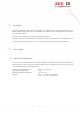
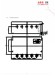
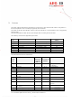
pin configuration of the PCB
X1
X2
X3
X4
X5
shielding
ground
TXD
RXD
1
2
3
4
5
6
make contact of relay QN1
1
2
3
4
5
data
shielding of data
sync
ground
12V
break contact of relay
QN1
1
2
1
2
24V
ground
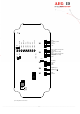
LED1 - antenna
LED2 - no read
LED3 - read
LED4 - dig-input
LED5 - error
LED6 - power
LED7 - RxD
LED8 - TxD
LED9 - not used
relay QN1
make contact of relay QR1
relay QR1
break contact of relay
QR1
digital input +
digital input
On
1 2 3 4 5 6 7 8
DIP-Switch
TP4
JP5
JP1
JP2
JP3
JP4
+12V GND
3
4
1
2