
User manual


27 Chapter 3
FIFO Enable/Disable (JP6)
When you enable the PCL-818HD/HG 's FIFO (First In First Out) buffer,
each time the card makes an A/D reading, it will store the data in both the
A/D output registers (accessed at addresses BASE+0/1) and in the FIFO
buffer (accessed at BASE+23/24). When you enable the FIFO, the PCL-
818HD/HG will require 32 consecutive I/O addresses.
When you disable the FIFO buffer, you can only access the converted
data from the A/D output registers at BASE+O/1. The PCL-818HD/HG
will only require 16 consecutive VO addresses.
Table 3-6: Jumper JP6 Settings
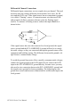
Ext. Trigger and Counter Gate 0 Control (JP5)
JP5 has two jumpers. The upper jumper selects the card's A/D trigger
source when you use external triggering. The lower jumper selects the
gate control for counter 0 of the card's 8254 timer/counter.
Table 3-7: Jumper Settings
Jumpers Function Description
JP6 Disabled
Enabled (default)
Jumpers Function Description
JP5 (Upper) G0 (default)
DI2
JP5 (Lower) Ext. (default)
DI0