
User manual


PCI-7020 User Manual 28
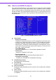
3.5 Advanced Chipset Features
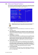
By choosing the “Advanced Chipset Features” option from the “Initial Setup Screen”
menu, the screen below will be displayed. This sample screen contains the manufac-
turer’s default values for the PCI-7020, as shown in Figure 3.4:
Figure 3.4 Advanced chipset features screen
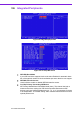
! DRAM Timing Selectable
This item allows you to control the DRAM speed. The selections are “Manual” or
“By SPD”.
! CAS Latency Time
When DRAM Timing Selectable is set to [Manual], this field is adjustable. This
controls the CAS latency, which determines the time interval between SDRAM
starting a read command and receiving it. The options are [3T], [4T], [5T], [6T]
and [Auto].
! DRAM RAS# to CAS# Delay
When DRAM Timing selectable is set to [Manual], this field is adjustable. When
DRAM is refreshed, the rows and columns are addressed separately. This setup
item allows users to determine the timing of the transition from RAS (row
address strobe) to CAS (column address strobe). The less the clock cycles are,
the faster the DRAM speed is. Setting options are [2T] to [6T], and [Auto].
! DRAM RAS# Precharge
When the DRAM Timing Selectable is set to [Manual], this field is adjustable.
This setting controls the number of cycles for Row Address Strobe (RAS) to be
allowed to precharge. If sufficient time has not been allowed for the RAS to
accumulate its charge before DRAM refresh, refreshing may be incomplete and
DRAM may fail to retain data. This item applies only when synchronous DRAM
is installed in the system. Setting options are [2T] to [6T], and [Auto].
! Precharge Delay (RAS)
This item allows you to select the value in this field, depending on whether the
board has paged DRAMs or EDO (extended data output) DRAMs. The choices
are: “4” to “15” and “Auto”.
Note! DRAM default timings have been carefully chosen and should ONLY be
changed if data is being lost. Please first contact technical support.