PCI-1720 4-ch Isolated Analog Output Card PCI-1720U 4-ch Isolated Analog Output Card with Universal PCI Bus User Manual
Copyright This documentation and the software included with this product are copyrighted 2005 by Advantech Co., Ltd. All rights are reserved. Advantech Co., Ltd. reserves the right to make improvements in the products described in this manual at any time without notice. No part of this manual may be reproduced, copied, translated or transmitted in any form or by any means without the prior written permission of Advantech Co., Ltd. Information provided in this manual is intended to be accurate and reliable.
Product Warranty (2 years) Advantech warrants to you, the original purchaser, that each of its products will be free from defects in materials and workmanship for two years from the date of purchase. This warranty does not apply to any products which have been repaired or altered by persons other than repair personnel authorized by Advantech, or which have been subject to misuse, abuse, accident or improper installation.
CE Notification PCI-1720 and PCI-1720U have passed the CE test for environmental specifications when shielded cables are used for external wiring. We recommend the use of shielded cables. This kind of cable is available from Advantech. Please contact your local supplier for ordering information. Technical Support and Assistance Step 1. Visit the Advantech web site at www.advantech.com/support where you can find the latest information about the product. Step 2.
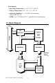
Contents Chapter 1.1 1.2 1.3 1.4 1.5 Chapter 1 General Information ....................................... 2 Introduction ................................................................................. Features........................................................................................ Applications................................................................................. Specifications............................................................................... Block Diagram........
Table 3.2: Identity Register of PCI-1720U ........................... 21 Chapter 4 Register Structure and Format.................... 24 4.1 Overview ................................................................................... 24 4.2 I/O Port Address Map................................................................ 25 Table 4.1: Register Format and Function Description .......... 25 4.2.1 D/A Output Channel 0 to 3 ..................................................... 26 Table 4.
1 CHAPTER 2 General Information
Chapter 1 General Information 1.1 Introduction PCI-1720 cards are isolated analog output cards. They provide four 12-bit analog output channels with isolation protection of 2,500 V DC between the outputs and the PCI bus. This is ideal for industrial applications where high-voltage protection is required. PCI-1720U is also equipped with a universal PCI interface.
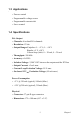
1.3 Applications • Process control • Programmable voltage source • Programmable current sink • Servo control 1.4 Specifications D/A Output • Channels: 4 isolated D/A channels • Resolution: 12 bits • Output Ranges:Unipolar: 0 ~ +5 V, 0 ~ +10 V Bipolar: ±5 V, ±10 V Current loop (sink): 0 ~ 20 mA, 4 ~ 20 mA • Throughput: 500 kHz • Accuracy: ±0.024% • Isolation Voltage: 2,500 V DC between the outputs and the PCI bus • Output Current: ±5 mA max. • Current Loop Excitation Voltage: 50 V max.
Environment • Operating Temperature: 0 ~ 60° C (32 ~ 140° F) • Storage Temperature: -20 ~ 70° C (-4 ~ 158° F) • Operating Humidity: 5 ~ 95 % RH non-condensing (refer to IEC 68-2-3) • MTBF: over 71,280 hrs @ 25° C, grounded, fixed environment 1.
CHAPTER 2 2 Installation This chapter gives users a package item checklist, proper instructions for unpacking and step-by-step procedures for both driver and card installation.
Chapter 2 Installation 2.1 Unpacking After receiving your PCI-1720 package, please inspect its contents first. The package should contain the following items: • PCI-1720 or PCI-1720U card • Companion CD-ROM (Device Drivers included) • User Manual PCI-1720 cards harbors certain electronic components vulnerable to electrostatic discharge (ESD). ESD can easily damage the integrated circuits and certain components if preventive measures are ignored.
• Whenever you handle the card, grasp it only by its edges. DO NOT TOUCH the exposed metal pins of the connector or the electronic components. Note: Keep the anti-static bag for future use. You might need the original bag to store the card if you have to remove the card from PC or transport it elsewhere. 2.2 Driver Installation We recommend you to install the driver before you install the PCI-1720 card into your system, since this will guarantee a smooth installation process.
Note: If the autoplay function is not enabled on your computer, use Windows Explorer or Windows Run command to execute SETUP.EXE on the companion CDROM. Step 3: Select the Individual Driver option. Step 4: Select the specific device then just follow the installation instructions step by step to complete your device driver installation and setup. Figure 2.
2.3 Hardware Installation Make sure you have installed the driver first before you install the card (please refer to 2.2 Driver Installation). After the Device Drivers installation is completed, you can then install the PCI-1724U card into any PCI slot on your computer. However, it is suggested that you refer to the computer user’s manual or related documentation if you have any doubt. Please follow the steps below to install the card onto your system. 1.
After the PCI-1724U card is installed, you can verify whether it is properly installed on your system in the Device Manager: 1. Access the Device Manager through Control Panel/System/Device Manager. 2. The device name of the PCI-1724U should be listed on the Device Manager tab on the System Property Page. Figure 2.3: The Device Name Listed on the Device Manager If your card is properly installed, you should see the device name of your card listed on the Device Manager tab.
2.4 Device Setup and Configuration The Advantech Device Manager program is a utility that allows you to set up, configure and test your device, and later stores your settings on the system registry. These settings will be used when you call the APIs of Advantech Device Drivers. 2.4.1 Setting Up the Device 1. To install the I/O device for your card, you must first run the Device Installation program (by accessing Start/Programs/ Advantech Automation/Device Manager). 2.
2.4.2 Configuring the Device 3. In the Device Setting dialog box (Fig.2-5), you can calibrate the voltage output range for the 8 D/A channels in 4 groups. For more detailed information, please refer to Appendix D Calibration Utility. Figure 2.5: The Device Setting dialog box Note: Users have three options for the output voltage ranges and current ranges: -10 ~ 10 V, 0 ~ 20 mA and 4 ~ 20 mA.
4. After you have finished configuring the device, click OK and the device name will appear in the Installed Devices box as seen below: Figure 2.6: Device Name Appearing on the List of Devices Box After your card is properly installed and configured, you can click the Test… button to test your hardware by using the testing utility supplied. For more detailed information, please refer to Chapter 2 of the Device Drivers Manual. You can also find the rich examples on the CD-ROM to speed up your programming.
PCI-1720 & 1720U User Manual 14
CHAPTER 3 2 Jumpers and I/O Connectors
Chapter 3 Jumpers and I/O Connectors PCI-1720 cards are Plug & Play compatible, i.e. the system BIOS assigns the system resources such as the base address and the interrupt number automatically. There are only 2 functions with 5 jumpers to configure to your applications requirements. The following sections offer the necessary information for setting the PCI-1720 card’s jumpers. You may need to refer to the figure below for help in identifying jumper locations. Figure 3.
Note! In order to maintain accurate outputs for your field applications, it is important that you calibrate the PCI-1720U’s variable resistors (VRs) from time to time. Calibration instructions are provided in Appendix A. 3.1.2 Jumper JP5 Setting for the Reset State Jumper JP5 gives the PCI-1720U a new and valuable capability. With JP5 enabled, the PCI-1720U “memorizes” all D/A output settings and output values, and, in the event of a “hot” reset, i.e.
3.2 Connector and Pin Assignments PCI-1720 cards use one DB-37 female connector, which is located on the card at CN1 (see Figure 3-1) and connects D/A signals to external devices. The following figure shows the pin assignments of the connector.
3.2.1 Signal Descriptions of I/O Connector Signal Name Reference Direction VOUT<0...3> AGND Output Analog Voltage Output Channels 0 through 3. These pins supply the voltage outputs for the analog outputs. ISINK<0...3> AGND Input Current Sink Channels 0 through 3. These pins provide the current loop sink input. +12 V OUT AGND Output +12 VDC Source. This pin is a +12 V DC power supply (80mA max.) for current loop exciting voltage. AGND - - Analog Ground.
3.3 Setting the BoardID Switch (SW1) BoardID settings are used to get the board’s unique identifier. The PCI1720 cards have a built-in DIP switch (SW1), which is used to define each card's unique identifier. You can determine the unique identifier in the register as shown in Table 3.2. When there are multiple identical cards in the same chassis, the BoardID switch helps differentiating the boards by identifying each card's device number with the switch setting.
3.3.1 Identity Register You can determine the identity in the register as shown in the table below. Table 3.
PCI-1720 & 1720U User Manual 22
4 CHAPTER 2 Register Structure and Format
Chapter 4 Register Structure and Format 4.1 Overview PCI-1720 cards are delivered with an easy-to-use 32-bit DLL driver for user programming under Windows 98, 2000 and XP operating systems. We advise users to program the card using the 32-bit DLL driver provided by Advantech to avoid the complexity of low-level programming by register. The most important consideration in programming the PCI-1720 cards at register level is to understand the function of the card’s registers.
4.2 I/O Port Address Map PCI-1720 cards require 12 addresses in the PC’s I/O space. The address of each register is specified as an offset from the card’s base address. For example, BASE + 0 is the card’s base address and BASE + 7 is the base address plus seven bytes. Table 4.1 shows the function of each register and its address relative to the card’s base address Table 4.
4.2.1 D/A Output Channel 0 to 3 The write-only registers of BASE + 2(n) and BASE + (2(n) + 1) accept data for D/A output channel n (n = 0, 1, 2, 3) Table 4.2: Register for D/A Data Base Address + decimal Data 7 6 5 4 3 2 1 0 +2(n) D7 D6 D5 D4 D3 D2 D1 D0 D11 D10 D9 D8 +(2(n)+1) Function Description R/W D/A output channel n W D11 ~ D0 Digital to Analog data. D0 is the LSB (Least Significant Bit) and D11 is the MSB (Most Significant Bit) of the D/A data.
4.2.3 Synchronized Output Prompt Register During normal operation, the card will accept digital values one at a time from the host PC, convert these values to analog values, and immediately output these analog values from the channels directed by the host PC. However, the cards have the capability to store each analog value in its proper channel buffer as it is generated, then simultaneously output one analog value from each of its four channels on receipt of a synchronizing character.
4.3 Unipolar and Bipolar Binary Code Tables Table 4.6: Unipolar Binary Code Table Digital Input Code MSB Examples of Analog Output Voltage LSB 1111 1111 1000 0000 0001 Vref (2049/4096) 1000 0000 0000 Vref (2048/4096) 0111 1111 0000 0000 0001 Vref (1/4096) 0000 0000 0000 Vref (0/4096) Notes: 1111 Vref (4095/4096) 1111 Vref (2048/4096) 1. Vref is the reference source voltage that you selected. Vref is +5 V or +10 V. 2. Nominal full scale is given by FS = Vref ( (4095/4096). 3.
5 CHAPTER 2 Signal Connections
Chapter 5 Signal Connections 5.1 Overview Making correct signal corrections is important for accurate data transmissions. Since most data acquisition applications involve some form of voltage measurement, making a sound signal connection will also protect your equipment against possible damage. This chapter shows you how to make proper signal connections. 5.2 D/A Voltage Output Connections PCI-1720 cards support four channels of D/A voltage output. Only one output signal wire is used with each channel.
Internal Side External Side VOUT D/A Grounded Load AGND Figure 5.2: Grounded-load Connection for D/A Voltage Output Internal Side External Side VOUT D/A Diff. Load with Ground AGND Figure 5.
5.3 Current Sink Connections The PCI-1720 cards’ current loop output uses a 0 to +5 V (unipolar) voltage output as each channel’s driving source. Current drive circuits consist of a power field-effect transistor (FET). The current output’s voltage bias must be less then 50 V for accurate results. The card also provides an internal +12 V power source for current loop excitation. You can use three types of current sink connections: 1. Grounded load with a floating power supply. 2.
Internal Side External Side ISINK 0 ~ 20 mA or 4 ~ 20 mA Floating Load AGND +12 VDC Figure 5.6: Floating-load Conn. with an Internal +12 VDC Power Supply 5.4 Current Sink Load and Power Supply You have to select the current sink load and power supply carefully. The current sink circuitry of the PCI-1720 cards is as shown below. Internal Side 0~5V or 1~5V { + - External Side PD 0 ~ 20 mA or 4 ~ 20 mA RL 249 Ω + - Vs AGND Figure 5.
where VS: Power supply voltage of current sink. RL: Load of current sink. PD: Power dissipation of FET. When you determine VS and RL, three conditions must be satisfied. VS > (RL + 249) ( 0.02) VS £ 50 PD = (VS - (RL + 249) x 0.02) x 0.02 < 0.2 Example 1 If you use the internal power supply VS = +12 V, RL must be less than 351 W (12 / 0.02 - 249 > RL). Select RL = 200 W, PD = 0.0604 < 0.2 OK! Example 2 If you use the external power supply VS = +40 V, RL must be less than 1.75 kW (40 / 0.02 - 249 > RL).
APPENDIX A 2 Calibration This appendix provides brief information on PCI-1720 cards calibration. Regular calibration checks are important to maintain accuracy in data acquisition and control applications.
Appendix A Calibration A.1 Overview PCI-1720 cards are calibrated at the factory for initial use. However, a recalibration of the analog analog outputs is recommended: 1. Every six months. 2. Everytime the analog output range is changed. We provide a calibration program on the companion CD-ROM. The calibration programs make calibration easier.
A.2 Starting Calibration PCI-1720 cards use eight variable resistors (VRs), two for each channel, which allow you to calibrate each of the card’s four output channels. The following information outlines the function of each VR. Refer to the illustration shown below for the locations of the VRs. Figure A.1: PCI-1720U VR assignment VR1 Channel 0’s full scale (gain) adjustment. VR2 Channel 1’s full scale (gain) adjustment. VR3 Channel 2’s full scale (gain) adjustment.
A.3 Unipolar Output Calibration 1. Select an appropriate output range for the channel to be calibrated. 2. Set all digital input codes to 0. Then adjust VRn (n = 5, 6, 7, 8 depending on what channel is to be calibrated, see prior page) until your voltmeter’s reading is 0.000 volts. 3. Set all digital input codes to 1 (see Unipolar Binary Code Table in Section 4.3).