PCI-1713 32-channel Isolated Analog Input Card User's manual
Copyright This documentation and the software included with this product are copyrighted 1999 by Advantech Co., Ltd. All rights are reserved. Advantech Co., Ltd. reserves the right to make improvements in the products described in this manual at any time without notice. No part of this manual may be reproduced, copied, translated or transmitted in any form or by any means without the prior written permission of Advantech Co., Ltd. Information provided in this manual is intended to be accurate and reliable.
Contents CHAPTER 1 General Information ........................ 1 1.1 Introduction .......................................................... 2 1.2 Features................................................................ 3 1.3 Specifications ....................................................... 3 1.4 Block Diagram ..................................................... 6 CHAPTER 2 Installation ........................................ 7 2.1 Initial Inspection .................................................
.7 Control Register .................................................. 27 4.8 Status Register .................................................... 28 4.9 Clear Interrupt and FIFO .................................. 29 4.10 Programmable Timer/Counter Registers ......... 29 CHAPTER 5 Calibration ...................................... 31 5.1 Introduction ......................................................... 32 5.2 VR Assignment .................................................... 32 5.3 A/D Calibration ...
CHAPTER 1 General Information Chapter 1 General Information 1
1.1 Introduction The PCI-1713 is a 12-bit 32-channel analog input card for the PCI bus. It provides 32 analog input channels with a sampling rate up to 100k samples/s, 12-bit resolution and isolation protection of 2500 VDC. PCI-bus Plug and Play The PCI-1713 uses a PCI controller to interface the card with the PCI bus. The controller fully implements the PCI bus specification Rev 2.1. All bus relative configurations, such as base address and interrupt assignment, are automatically controlled by software.
Satisfies the Need for Isolation Protection The PCI-1713 provides optical isolation protection of 2500 VDC between the inputs and the PC bus to protect the PC and peripherals from damage due to high voltages on the input lines. It is ideal for the situations where budget-conscious users require flexibility, stability and a high level of isolation protection for their data acquisition system. 1.
• Maximum Input Overvoltage: ±30 V • Common Mode Rejection Ratio (CMRR) Gain CMRR 0.5, 1 75dB 2 80dB 4 84dB 8 84dB • Maximum sampling rate: 100 kHz • Accuracy: (depending on gain) Gain Accuracy 0.5, 1 0.01% of FSR±1LSB 2 0.02% of FSR±1LSB 4 0.02% of FSR±1LSB 8 0.
General: • I/O Connector: 37-pin D-type female connector • Dimensions: 175 mm x 100 mm (6.9” x 3.9”) • Power consumption: +5 V @ 850 mA (Typical), +5 V @ 1.0 A (Max.
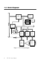
1.4 Block Diagram PCI Target Controller Address Decoder Address Bus Counter 1 PCI Bus INT 10 MHz OSC Counter 2 Pacer INT Generator Data Bus Channel Code ADC Control Logic EXT_TRG Gain Code Generator Isolation Isolation Channel Code Generator Isolation Isolation 12 bit A/D Converter + PGIA Figure 1-1: PCI-1713 block diagram 6 PCI-1713 User's Manual Multiplexer 32 S.E.
CHAPTER 2 Installation Chapter 2 Installation 7
2.1 Initial Inspection Before installing the PCI-1713, check the card for visible damage. We have carefully inspected the card both mechanically and electrically before shipment. It should be free of marks and in perfect order upon receipt. As you unpack the PCI-1713, check it for signs of shipping damage (damaged box, scratches, dents, etc.). If it is damaged or fails to meet specifications, notify our service department or your local sales representative immediately.
2.3 Installation Instructions The PCI-1713 can be installed in any PCI slot in the computer. However, refer to the computer user's manual to avoid any mistakes and danger before you follow the installation procedure below: 1. Turn off your computer and any accessories connected to the computer. Warning! TURN OFF your computer power supply whenever you install or remove any card, or connect and disconnect cables. 2. Disconnect the power cord and any other cables from the back of the computer. 3.
10 PCI-1713 User's Manual
CHAPTER 3 Signal Connections Chapter 3 Signal Connections 11
3.1 Overview Correct signal connections are one of the most important factors in ensuring that your application system is sending and receiving data correctly. A good signal connection can avoid much unnecessary and costly damage to your valuable PC and other hardware devices. This chapter will provide some useful information about how to connect analog input signals to the PCI-1713 card via the I/O connector. 3.
I/O Connector Signal Descriptions Signal Name Reference Direction AI<0…31> GND Input Analog Input Channels 0 through 31. Each channel pair, AI (i = 0, 2, 4...30), can be configured as either two single-ended inputs or one differential input. - Ground. These pins are the reference points for single-ended measurements and the bias current return point for differential measurement. GND EXT_TRG - GND Input Description A/D External Trigger.
3.3 Analog Input Connections This section continues to describe how to make analog input signal connections to the PCI-1713 card via the I/O connector. Single-ended Channel Connections The single-ended input configuration has only one signal wire for each channel, and the measured voltage (Vm) is the voltage of the wire referred to the common ground. A signal source without a local ground is also called a “floating source”. It is fairly simple to connect a single-ended channel to a floating signal source.
Differential Channel Connections The differential input configuration has two signal wires for each channel, and the differential input responds only to voltage differences between High and Low inputs. On the PCI-1713 card, when all channels are configured to differential input, up to 16 analog channels are available. If one side of the signal source is connected to a local ground, the signal source is ground-referenced.
If a floating signal source is connected to the differential input channel, the signal source may exceed the common-mode signal range of the PGIA, and the PGIA will be saturated with erroneous voltage-readings. You must therefore reference the signal source to the AIGND. Figure 3-4 shows a differential channel connection between a floating signal source and an input channel on the PCI-1713 card. In this figure, each side of the floating signal source is connected through a resistor to the AIGND.
External Trigger Source Connection In addition to pacer triggering, the PCI-1713 card also allows external triggering for A/D conversions. A low-to-high edge coming from EXT_TRG will trigger an A/D conversion on the PCI-1713 board. Note!: Don't connect any signal to the EXT_TRG pin when the external trigger function is not being used.
• Make sure that your signal lines do not travel through conduits, because these may contain power lines. Also, keep your signals far from electric motors, breakers or welding equipment, as these can create magnetic fields. • Keep a reasonable distance between high-voltage (or high-current) lines and signal cables connected to the PCI-1713 card if the cables run parallel, or route signal cables at right angles to high voltage/current cables.
CHAPTER 4 Register Structure and Format Chapter 4 Register Structure and Format 19
4.1 Overview The PCI-1713 is delivered with an easy-to-use 32-bit DLL driver for user programming under the Windows 98/95/NT operating system. We advise users to program the PCI-1713 using the 32-bit DLL driver provided by Advantech to avoid the complexity of low-level programming by register. The most important consideration in programming the PCI-1713 card at a register level is to understand the function of the card’s registers.
Table 4-1: PCI-1713 register format (Part 1) Base Address + decimal Read 7 6 5 4 3 2 1 0 Channel Number and A/D Data 1 0 AD7 AD6 AD5 AD4 AD11 AD10 AD9 AD8 AD3 AD2 AD1 AD0 N/A 3 2 N/A 5 4 Status Register 7 6 ONE/FH IRQEN IRQ F/F F/H F/E GATE EXT PACER SW D2 D1 D0 D2 D1 D0 D2 D1 D0 N/A 9 8 Counter 0 25 24 D7 D6 D5 D4 D3 Counter 1 27 26 D7 D6 D5 D4 D3 Counter 2 29 28 D7 D6 D5 D4 D3 N/A 31 30 Chapter 4 Register Structure and Format 21
Table 4-1: PCI-1713 register format (Part 2) Base Address + decimal Write 7 6 5 4 3 2 1 0 G1 G0 PACER SW D2 D1 D0 D2 D1 D0 D2 D1 D0 D2 D1 D0 Software A/D Trigger 1 0 A/D Channel Range Setting 3 2 S/D B/U G2 MUX Control 5 Stop channel 4 Start channel Control Register 7 6 ONE/FH IRQ GATE EXT Clear Interrupt and FIFO 9 clear FIFO 8 clear interrupt Counter 0 25 24 D7 D6 D5 D4 D3 Counter 1 27 26 D7 D6 D5 D4 D3 Counter 2 29 28 D7 D6 D5 D4 D3 Counter Cont
4.3 A/D Data BASE+0 and BASE+1 These two bytes, BASE+0 and BASE+1, hold the result of A/D conversion data. The 12 bits of data from the A/D conversion are stored in BASE+1 bit 3 to bit 0 and BASE+0 bit 7 to bit 0.
Table 4-3: Register for A/D channel range setting Write Bit # A/D channel range setting 7 6 BASE+2 S/D 5 4 S/D B/U 3 2 1 0 G2 G1 G0 Single-ended or Differential 0 means the channel is single-ended, and 1 means it is differential. B/U Bipolar or Unipolar 0 means the channel is bipolar, and 1 means it is unipolar.
4.6 MUX ControlBASE+4 and BASE+5 Table 4.5: The register for multiplexer control Write Bit # MUX Control 7 6 5 4 3 2 1 0 BASE+5 CH4 CH3 CH2 CH1 CH0 BASE+4 CL4 CL3 CL2 CL1 CL0 CL4 ~ CL0 Start Scan Channel Number CH4 ~ CH0 Stop Scan Channel Number BASE+4 bit 4 to bit 0, CL4 ~ CL0, act as a pointer when you program the A/D channel setting (see previous section). When you set the MUX start channel to an analog input channel, AIn ( n = 0, 1, 2, 3,...
Example 1 If the start scan input channel is AI3 and the stop scan input channel is AI7, then the scan sequence is AI3, AI4, AI5, AI6, AI7, AI3, AI4, AI5, AI6, AI7, AI3, AI4… Example 2 If the start scan channel is AI29 and the stop scan channel is AI2, then the scan sequence is AI29, AI30, AI31, AI0, AI1, AI2, AI29, AI30, AI31, AI0, AI1, AI2, AI29, AI30… This scan logic of the PCI-1713 card is quite powerful and easily understood. You can respectively set the gain code, B/U and S/D, for each channel.
4.7 Control Register BASE+6 The write-only register BASE+6 allows users to set an A/D trigger source and an interrupt source. Table 4-6: Control register Write Control Register Bit # 7 BASE + 6 6 5 4 ONE/FH IRQEN 3 2 1 0 GATE EXT PACER SW SW Software trigger enable bit Set 1 to enable software trigger, and set 0 to disable. PACER PACER trigger enable bit Set 1 to enable pacer trigger, and set 0 to disable.
4.8 Status Register BASE+6 and BASE+7 The registers of BASE+6 and BASE+7 provide information for the A/D configuration and operation. Table 4-7: Status register Read Status Register Bit # 7 6 5 4 BASE+7 BASE+6 ONE/FH IRQEN 3 2 1 0 IRQ F/F F/H F/E GATE EXT PACER SW The content of the status register of BASE+6 is the same as that of the control register. F/E FIFO Empty flag This bit indicates whether the FIFO is empty. 1 means that the FIFO is empty.
4.9 Clear Interrupt and FIFO BASE+8 and BASE+9 Writing data to either of these two bytes clears the interrupt or the FIFO. Table 4-8: Registers to clear interrupt and FIFO Write Bit # Clear Interrupt and FIFO 7 6 5 4 3 BASE+9 Clear FIFO BASE+8 Clear Interrupt 2 1 0 4.10 Programmable Timer/Counter Registers BASE+24, BASE+26, BASE+28 and BASE+30 The four registers of BASE+24, BASE+26, BASE+28 and BASE+30 are used for the 82C54 programmable timer/counter.
30 PCI-1713 User's Manual
CHAPTER 5 Calibration Chapter 5 Calibration 31
5.1 Introduction Regular calibration checks are important to maintain accuracy in data acquisition and control applications. To assist users in the A/D calibration process, we provide one calibration program, ADCAL.EXE, on the PCI-1713 software CD-ROM. The ADCAL.EXE program makes A/D calibrations easy. It leads you through the calibration and setup procedure with a variety of prompts and graphic displays, showing you all of the correct settings and adjustments.
Figure 5-1: PCL-1713 VR assignment The following list shows the function of each VR: VR VR1 Function A/D full scale (gain) VR2 A/D bipolar offset VR3 A/D unipolar offset VR4 PGIA initial offset TP1 PGIA output 5.3 A/D Calibration Regular and accurate calibration procedures ensure the maximum possible accuracy. The ADCAL.EXE calibration program leads you through the whole A/D offset and gain adjustment procedure. The basic steps are outlined below: 1.
10. Adjust VR1 until the output codes from the card's AI0 flickers between 4094 and 4095. 11. Repeat step 7 to step 10, adjusting VR2 and VR1. 12. Connect a DC voltage source with value equal to 2047.5 LSB (4.9959 V) to AI1. 13. Adjust VR3 until the output codes from the card's AI1 flickers between 2047 and 2048. A/D code 34 Mapping Voltage Hex. Dec. Bipolar ± 5V Unipolar 0 to 10V 000h 0 -4.9971V 0V 7FFh 2047 -0.0024V 4.9947V 800h 2048 0V 4.9971V FFFh 4095 +4.9947V 9.
APPENDIX A 82C54 Counter Chip Functions Appendix A 8524 Counter Chip Functions 35
A.1 Introduction The PCI-1713 uses one Intel 82C54 compatible programmable interval timer/counter chip. This popular 82C54 offers three independent 16-bit counters, counter 0, counter 1 and counter 2. Counter 0 is not available for users. Counter 1 is cascaded with counter 2 to create a 32-bit timer for the pacer trigger. A low-to-high edge of counter 2 output can trigger an A/D conversion, and users can utilize this signal as a synchronous signal for other applications. A.
Description: SC1 & SC0 Select counter.
If you set the module for binary counting, the count can be any number from 0 up to 65535. If you set it for BCD (Binary Coded Decimal) counting, the count can be any number from 0 to 9999. If you set both SC1 and SC0 bits to 1, the counter control register is in read-back command mode. The control register data format then becomes: BASE + 30(Dec) 82C54 control, read-back mode Bit D7 D6 D5 D4 D3 D2 D1 D0 Value X 1 1 C N T S TA C2 C1 C0 CNT = 0 Latch count of selected counter(s).
A.3 Counter Operating Modes MODE 0 Stop on Terminal Count The output will initially be low after you set this mode of operation. After you load the count into the selected count register, the output will remain low and the counter will count. When the counter reaches the terminal count, its output will go high and remain high until you reload it with the mode or a new count value. The counter continues to decrement after it reaches the terminal count.
MODE 3 Square Wave Generator This mode is similar to Mode 2, except that the output will remain high until one half of the count has been completed (for even numbers), and will go low for the other half of the count. This is accomplished by decreasing the counter by two on the falling edge of each clock pulse. When the counter reaches the terminal count, the state of the output is changed, the counter is reloaded with the full count and the whole process is repeated.
A.4 Counter Operations Read/Write Operation Before you write the initial count to each counter, you must first specify the read/write operation type, operating mode and counter type in the control byte and write the control byte to the control register [BASE + 30(Dec)]. Since the control byte register and all three counter read/write registers have separate addresses and each control byte specifies the counter it applies to (by SC1 and SC0), no instructions on the operating sequence are required.
Counter Latch Operation Users often want to read the value of a counter without disturbing the count in progress. You do this by latching the count value for the specific counter then reading the value. The 82C54 supports the counter latch operation in two ways. The first way is to set bits RW1 and RW0 to 0. This latches the count of the selected counter in a 16-bit hold register. The second way is to perform a latch operation under the read-back command. Set bits SC1 and SC0 to 1 and CNT = 0.
APPENDIX B PCLD-881B Wiring Terminal Board Appendix B PCLD-881B Wiring Terminal Board 43
B.1 Introduction The PCLD-881B Screw-terminal Board provides convenient and reliable signal wiring for the PCI-1713 and PCL-813B, both of which have a 37-pin D-type connector. Due to its special PCB layout you can install passive components to construct your own signal-conditioning circuits. The user can easily construct a low-pass filter, attenuator or current shunt converter by adding resistors and capacitors on to the board's circuit pads. B.
B.
B.5 Single-ended Connections RAn AIn RBn Cn AIGND Internal side Field side a) Straight-through connection (factory setting) RAn = 0 Ω (short) RBn = none Cn = none b) 1.6 kHz (3dB) low pass filter RAn = 10 kΩ RBn = none Cn = 0.01µF f3dB = 1 2 πR A n C n c) 10 : 1 voltage attenuator: RAn = 9 kΩ RBn = 1 kΩ Cn = none Attenuation = where n = 0, 1, 2, .....
B.6 Differential Connections RAn RDn AIn CDn AIn+1 where n = 0, 2, 4, ....., 30 RAn+1 Internal side Field side a) Straight-through connection (factory setting): RAn = 0 Ω (short) RAn+1 = 0 Ω (short) RDn = none CDn = none b) 1.6 kHz (3dB) low pass filter RAn = 5 kΩ RAn+1 = 5 kΩ RDn = none CDn = 0.01µF f3dB = 1 2 π( R A n + R A n + 1 ) C D n c) 10 : 1 voltage attenuator: RAn = 4.5 kΩ RAn+1 = 4.
B.
CN1 39 EX T _T RG 19 A I31 37 A I30 18 A I29 36 A I28 17 A I27 35 A I26 16 A I25 34 A I24 15 A I23 33 A I22 14 A I21 32 A I20 13 A I19 31 A I18 12 A I17 30 A I16 11 GND 29 GND 10 GND 28 GND 9 A I15 27 A I14 8 A I13 26 A I12 7 A I11 25 A I10 A I9 6 24 A I8 5 A I7 23 A I6 4 A I5 22 A I4 3 A I3 21 A I2 2 A I1 20 A I0 1 38 C O N N E C T O R D B 37 JP 1 3 EX T _T RG 2 1 JU M P 3 X 1 Appendix B PCLD-881B Wiring Terminal Board 49
50 PCI-1713 User's Manual