
Specifications


Appendix D
– 94 –PCI-1710 series User’s Manual
Advantech Co., Ltd.
www.advantech.com
D.2 Counter Read/Write and Control Registers
The 82C54 programmable interval timer uses four registers at addresses
BASE + 24(Dec), BASE + 26(Dec), BASE + 28(Dec) and
BASE + 30(Dec) for read, write and control of counter functions.
Register functions appear below:
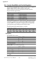
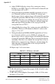
Register Function
BASE + 24 (Dec) Counter 0 read/write
BASE + 26 (Dec) Counter 1 read/write
BASE + 28 (Dec) Counter 2 read/write
BASE + 30 (Dec) Counter control word
Since the 82C54 counter uses a 16-bit structure, each section of read/
write data is split into a least significant byte (LSB) and most signifi-
cant byte (MSB). To avoid errors it is important that you make read/
write operations in pairs and keep track of the byte order.
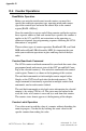
The data format for the control register is as below:
BASE+30(Dec) 82C54 control, standard mode
Bit D7 D6 D5 D4 D3 D2 D1 D0
Value SC1 SC0 RW1 RW0 M2 M1 M0 BCD
Description:
SC1 & SC0 Select counter
Counter SC1 SC0
0 0 0
1 0 1
2 1 0
Read-back command 1 1
RW1 & RW0 Select read/write operation
Operation RW1 RW0
Counter latch 0 0
Read/write LSB 0 1
Read/write MSB 1 0
Read/write LSB first, 1 1
then MSB