
Specifications

Auto-Optical Solder Inspection
SMT/PCB Industrial Assembly
Taiwan
11
Introduction
Printed Circuit Boards are used in virtually every electronic device today, from cellular phones
and personal computers to industrial and medical machinery. One of the most integral steps in
assembling Circuit Boards is the solder placement.
Our customer was having issues in the creation of their Circuit Boards with misplaced and weak
solder joints. Furthermore, they were using 2 separate machines for 2D solder inspection. To
save costs, increase reliability, and speed up the inspection process, the customer wanted
only 1 machine that could handle machine vision and control with 3D solder inspection
capabilities.
Project Requirements
Our customer was using an outdated system that
required 2 expensive machines, one for machine
vision and one for machine control. Furthermore, this
system was only capable of 2D solder inspection,
which is not good at judging the corners/angles of
the placement and can cause weak connections,
leading to faulty boards and potential short-circuits.
They desired to have an entirely new system, with
the following requirements:
•
They wanted 1 machine that could handle
both machine vision and control
•
The system needed to have 3D solder
inspection capabilities
•
They wanted a higher-performance PC-based
system
•
The system needed to have high inspection
accuracy with high-speed motion control
•
They wanted a system that required less
management
Solution Description
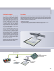
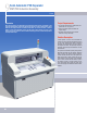
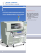
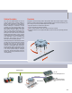
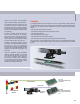
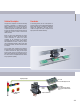
The system is comprised of an Optical
Inspection machine which examines
the surface of the PCB board. In the
machine architecture, there are 2
subsystems, one for moving the PCB
board and the other for visual quality
25