
User manual


Table Of Contents
- PCA-6011
- Contents
- 1 Hardware Configuration
- 1.1 Introduction
- 1.2 Features
- 1.3 Specifications
- 1.4 Jumpers and Connectors
- 1.5 Board Layout: Jumper and Connector Locations
- 1.6 PCA-6011 Block Diagram
- 1.7 Safety Precautions
- 1.8 Jumper Settings
- 1.9 System Memory
- 1.10 Memory Installation Procedures
- 1.11 Cache Memory
- 1.12 Processor Installation
- 1.13 Power Model Setting and Installation
- 1.14 ATX Mode
- 2 Connecting Peripherals
- 2.1 Introduction
- 2.2 IDE Connectors (IDE1)
- 2.3 Floppy Drive Connector (FDD1)
- 2.4 Parallel Port (LPT1)
- 2.5 VGA Connector (VGA1)
- 2.6 Serial Ports (COM1, COM2)
- 2.7 PS/2 Keyboard and Mouse Connector (KBMS1)
- 2.8 External Keyboard & Mouse (KBMS2)
- 2.9 CPU Fan Connector (CPUFAN1)
- 2.10 Front Panel Connectors (JFP1, JFP2, JFP3)
- 2.11 H/W Monitor Alarm (JOBS1)
- 2.12 LAN RJ45 connector (LAN1/LAN2)
- 2.13 HD Link connector (HDAUD1)
- 2.14 Serial ATA2 Interface (SATA1 ~ SATA4)
- 2.15 LAN LED connector (LAN LED1)
- 2.16 USB (USB12, USB34, USB56, USB78)
- 2.17 Case open (JCASE1)
- 3 AMI BIOS Setup
- 3.1 Introduction
- 3.2 Entering Setup
- 3.2.1 Main Setup
- 3.2.2 Advanced BIOS Features Setup
- 3.2.3 PCI/PNP Setup
- 3.2.4 Boot Settings
- 3.2.5 Security Settings
- 3.2.6 Advanced Chipset Settings
- 3.2.7 Exit Options
- 4 Chipset Software Installation Utility
- 5 VGA Setup
- 6 LAN Configuration
- A Programming the Watchdog Timer
- B I/O Pin Assignments
- B.1 IDE Hard Drive Connector (IDE1)
- B.2 Floppy Drive Connector (FDD1)
- B.3 Parallel Port Connector (LPT1)
- B.4 VGA Connector (VGA1)
- B.5 RS-232 Serial Port (COM1, COM2)
- B.6 PS/2 Keyboard/Mouse Connector (KBMS1)
- B.7 External Keyboard Connector (KBMS2)
- B.8 CPU Fan Power Connector (CPUFAN1)
- B.9 Power LED and Keyboard Lock Connector (JFP3 / PWR_LED & KEY LOCK)
- B.10 External Speaker Connector (JFP2 / SPEAKER)
- B.11 Reset Connector (JFP1 / RESET)
- B.12 HDD LED (JFP2 / HDDLED)
- B.13 ATX Soft Power Switch (JFP1 / PWR_SW)
- B.14 SM Bus Connector (JFP2/SNMP)
- B.15 HD Link connector (HDAUD1)
- B.16 LAN LED Connector (LAN LED1)
- B.17 AT Power Connector (ATXF1)
- B.18 H/W Monitor Alarm (JOBS1)
- B.19 USB Connector (USB12, USB34, USB56, USB78)
- B.20 Case Open Connector (JCASE1)
- B.21 GPIO Pin Header (GPIO1)
- B.22 System I/O Ports
- B.23 DMA Channel Assignments
- B.24 Interrupt Assignments
- B.25 1st MB Memory Map
- B.26 PCI Bus Map
41 PCA-6011 User Manual
Chapter 3
A
MI BIOS Setup
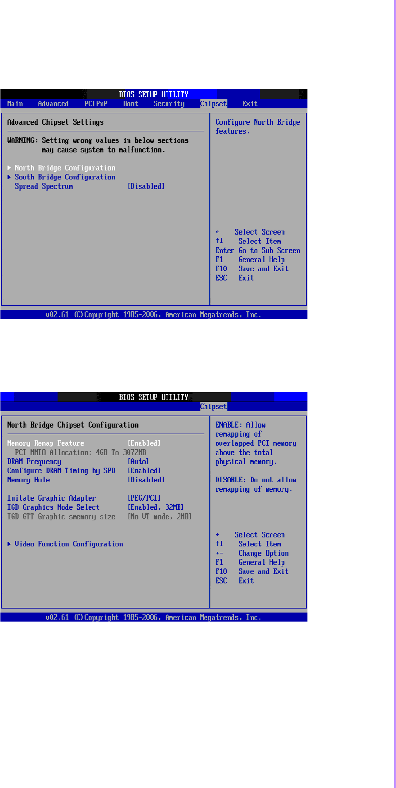
3.2.6 Advanced Chipset Settings
Figure 3.16 Advanced Chipset Settings
3.2.6.1 North Bridge Configuration
Allows user to set graphic and memory controller configurations.
Figure 3.17 North Bridge Configuration
Memory remap feature
The feature allows you to enable or disable the remapping of the overlapped
PCI memory above the total physical memory.
DRAM Frequency
Allows user to set DDR2 memory operating frequency.
Configure DRAM Timing by SPD
Allows user to set DRAM operating timing coefficients by SPD or Manual.
Memory hole