Copyright This documentation and the software included with this product are copyrighted 2002 by Advantech Co., Ltd. All rights are reserved. Advantech Co., Ltd. reserves the right to make improvements in the products described in this manual at any time without notice. No part of this manual may be reproduced, copied, translated or transmitted in any form or by any means without the prior written permission of Advantech Co., Ltd. Information provided in this manual is intended to be accurate and reliable.
Contents 1. INTRODUCTION.................................................................................................................. 1 1.1 FEATURES ........................................................................................................................ 1 1.2 APPLICATIONS ................................................................................................................. 4 1.3 INSTALLATION GUIDE ............................................................................
C.10 SOFTWARE LATCH — BASE+28H .............................................................................. 41 C.11 BOARD ID — BASE+28H.......................................................................................... 42 C.12 RESET COUNTER — BASE+2CH................................................................................ 43 C.13 DIGITAL OUTPUT — BASE+30H................................................................................ 44 C.14 DIGITAL INPUT/OUTPUT — BASE+30H ........
1. Introduction Thank you for buying the Advantech PCI-1784. The PCI-1784 is a 4axis quadrature encoder and counter card for PCI bus. This card includes four 32-bit quadruple AB phase encoder counters, 8-bit timer with multi range time-base selector and four isolated digital input and four isolated digital output. Its flexible interrupt sources are suitable for motor control and position monitoring.
Counters The PCI-1784 has four independent 32-bit counters. The maximum quadrature input rate is 2 MHz, and the maximum input rate in counter mode is 8 MHz. You can individually configure each counter for quadrature decoding, pulse/direction counting or up/down counting. Digital Input and Interrupts The PCI-1784 provides four digital input channels. Each channel accepts digital input as an index input for a rotary encoder or as a home sensor input for a linear encoder.
default configuration, depending on jumper setting. This practical function eliminates danger caused by miss-operation during unexpected system reset. Board ID The PCI-1784 has a built-in DIP Switch that helps define each card’s ID when multiple PCI-1784 cards have been installed on the same PC chassis. The board ID setting function is very useful when users build their system with multiple PCI-1784 cards.
1.2 Applications ❏ Motion control ❏ Position sensing, monitoring and measuring ❏ Coordinate measuring machines ❏ X-Y table monitors ❏ Robotics ❏ Machine control 1.
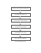
Install Driver from CD-ROM, then power-off PC Install Hardware and power-on PC Use driver utility to configure hardware Use test utility to test hardware Read examples & driver manual Start to write your own application Fig.
1.4 Software Overview Advantech offers a rich set of DLL drivers, third-party driver support and application software to help fully exploit the functions of your PCI1784 card: Device Drivers (on the companion CD-ROM) ❏ LabVIEW driver* ❏ Advantech ActiveDAQ ❏ Advantech GeniDAQ ❏ Programming choices for DA&C cards: You may use Advantech application software such as Advantech Device Drivers.
1.5 Device Drivers Programming Roadmap This section will provide you a roadmap to demonstrate how to build an application from scratch using Advantech Device Drivers with your favorite development tools such as Visual C++, Visual Basic, Delphi and C++ Builder. The step-by-step instructions on how to build your own applications using each development tool will be given in the Device Drivers Manual. Moreover, a rich set of example source codes are also given for your reference.
For information about using other function groups or other development tools, please refer to the Creating Windows 95/NT/2000 Application with Device Drivers chapter and the Function Overview chapter on the Device Drivers Manual. Programming with Device Drivers Function Library Advantech Device Drivers offers a rich function library to be utilized in various application programs.
1.6 Accessories Advantech offers a complete set of accessory products to support the PCI-1784 card. These accessories include: Wiring Cable ❏ PCL-10137H The PCL-10137H shielded cable is specially designed for PCI-1784 cards to provide high resistance to noise. To achieve a better signal quality, the signal wires are twisted in such a way as to form a “twisted-pair cable”, reducing cross-talk and noise from other signal sources.
2. Installation This chapter gives users a package item checklist, proper instructions about unpacking and step-by-step procedures for both driver and card installation. 2.1 Unpacking After receiving your PCI-1784 package, please inspect its contents first. The package should contain the following items: ! PCI-1784 card ! Companion CD-ROM (DLL driver included) ! User’s Manual The PCI-1784 card harbors certain electronic components vulnerable to electrostatic discharge (ESD).
Also pay extra caution to the following aspects to ensure proper installation: ! Avoid physical contact with materials that could hold static electricity such as plastic, vinyl and Styrofoam. ! Whenever you handle the card, grasp it only by its edges. DO NOT TOUCH the exposed metal pins of the connector or the electronic components. Note: ✎ Keep the anti-static bag for future use. You might need the original bag to store the card if you have to remove the card from PC or transport it elsewhere.
2.2 Driver Installation We recommend you to install the driver before you install the PCI1784 card into your system, since this will guarantee a smooth installation process. The Advantech Device Drivers Setup program for the PCI-1784 card is included on the companion CD-ROM that is shipped with your DA&C card package. Please follow the steps below to install the driver software: Step 1: Insert the companion CD-ROM into your CD-ROM drive.
Step 3: Select the Individual Drivers option. Step 4: Select the specific device then just follow the installation instructions step by step to complete your device driver setup. Fig. 2-2 Different options for Driver Setup For further information on driver-related issues, an online version of Device Drivers Manual is available by accessing the following path: Start/Programs/Advantech Device Drivers V2.0/Device Driver Manual 2.
Step 1: Turn off your computer and unplug the power cord and cables. TURN OFF your computer before installing or removing any components on the computer. Step 2: Remove the cover of your computer. Step 3: Remove the slot cover on the back panel of your computer. Step 4: Touch the metal part on the surface of your computer to neutralize the static electricity that might be on your body. Step 5: Insert the PCI-1784 card into a PCI slot. Hold the card only by its edges and carefully align it with the slot.
Fig. 2-3 The device name listed on the Device Manager Note: ✎ If your card is properly installed, you should see the device name of your card listed on the Device Manager tab. If you do see your device name listed on it but marked with an exclamation sign “!”, it means your card has not been correctly installed. In this case, remove the card device from the Device Manager by selecting its device name and press the Remove button. Then go through the driver installation process again.
2.4 Device Setup & Configuration The PCI-1784 Utility program is a utility that allows you to setup, configure and test your device, and later stores your settings on the system registry. These settings will be used when you call the APIs of Advantech Device Drivers. Board selection After your card is properly inserted, the Windows system will install the drivers properly. You just need to launch the PCI-1784 Utility for board selection.
Setting Up and configure the device Click Setup to configure each parameter. The dialog box will appear as seen below (Fig. 2-5): Fig.
Fig. 2-6 The “Operation” dialog box After your card is properly installed and configured, you can click the Operation button to test your hardware. For more detailed information, please refer to Chapter 2 of the Device Drivers Manual. You can also find the rich examples on the CD-ROM to speeding up your programming.
3. Signal Connections 3.1 Overview Maintaining signal connections is one of the most important factors in ensuring that your application system is sending and receiving data correctly. A good signal connection can avoid unnecessary and costly damage to your PC and other hardware devices. This chapter provides useful information about how to connect input and output signals to the PCI-1784 via the I/O connector. 3.
Setting the time to reset the digital outputs and the counter value Some users will want the capability of clearing each counter and the isolated digital output when the system (or PC) issues a reset signal on the PCI bus. Some users will want to clear their counter and digital output only as part of system power-on. The PCI-1784 satisfies both these needs by providing jumper JP2.
3.3 Signal Connections Pin Assignment Figure 3-2 shows the pin assignments for the 37-pin I/O connector on the PCI-1784. EGND 1 20 CH0A- CH0A+ 2 21 CH0B- CH0B+ 3 22 CH0Z- CH0Z+ 4 23 CH1A- CH1A+ 5 24 CH1B- CH1B+ 6 25 CH1Z- CH1Z+ 7 26 CH2A- CH2A+ 8 27 CH2B- CH2B+ 9 28 CH2Z- CH2Z+ 10 29 CH3A- CH3A+ 11 30 CH3B- CH3B+ 12 31 CH3Z- CH3Z+ 13 32 EGND IDI COM 14 33 IDI1 IDI0 15 34 IDI3 IDI2 16 35 EGND EGND 17 36 IDO1 IDO0 18 37 IDO3 IDO2 19 .
Quadrature encoder input Single ended outputs of Encoder CHnA+ CHnB+ CHnZ+ A B I PCI-1784 connector GND EGND A+ ADifferential B+ Boutputs of I+ Encoder or I- CHnA+ CHnACHnB+ CHnBCHnZ+ CHnZPCI-1784 connector EGND Line driver GND CHnA+ CHnB+ PULSE DIR Pulse/Direction Counter PCI-1784 connector GND EGND Figure 3-3: Quadrature encoder input connections 22
CHnA+ CHnB+ UP DN Up/Down Counter PCI-1784 connector GND EGND UP DN CHnA+ CHnB+ Two_Pulse Up Counter PCI-1784 connector GND EGND UP DN CHnA+ CHnB+ Two_Pulse Down Counter PCI-1784 connector GND EGND Figure 3-4: Quadrature encoder (up/down counter) input connections Note: ✎ In case you want to connect the Up/Down counter signal into the PCI-1784, be sure that all the signals must be connected. The floating connection will cause unexpected result.
Isolated digital input External Internal VCC IDI0~IDI3 DC (5-30V) GND IDI COM Figure 3-4: Isolated digital input connections Isolated digital output Internal External IDO0~IDO3 TTL level Isolated Protection Circuit TTL level EGND Figure 3-5: Isolated digital output connections 24
Appendix A. Specifications Encoder Output Number of Axis 4 (independent) Resolution 32-bit w/ Digital Filter 1.0 MHz Max. Quadrature w/o Digital Input Frequency 2.0 MHz Filter Digital Filter 4 stage Drive Type Single-ended or differential Counter Mode Quadrature, Up/Down, Count/Direction Optical Isolation 2500 VDC Max.
Interrupt Source Counter Latch Source General I/O Connector Type Dimensions Power Consumption Temperature Relative Humidity Certification Counter overflow, Counter underflow, Index input, Compare, Timer, Digital input Software, Timer, Index input, Digital input 37-pin D-sub female 175 mm x 100 mm (6.9" x 3.9") Typical Max.
Appendix B. Block Diagram C O U N TE R MODE C O N TR O L ADDRESS, CONTROL AND DATA BUS 32-B IT M U LTI-M O D E U P /D O W N C O U N TE R 32-B IT M U LTI-M O D E U P /D O W N C O U N TE R 32-B IT M U LTI-M O D E U P /D O W N C O U N TE R C H .0 P H A S E A C H .0 P H A S E B C H .0 IN D E X D IG ITA L FILT E R DIFF/SE ISOLA TION INPU T C IRCU IT 32-B IT U P /D O W N C O U N TE R C H .1 P H A S E A C H .1 P H A S E B C H .1 IN D E X C H .2 P H A S E A C H .2 P H A S E B C H .2 IN D E X C H .
28
Appendix C. Register Structure and Format C.1 Overview The PCI-1784 is delivered with an easy-to-use 32-bit DLL driver for user programming under the Windows 2000/95/98/NT/ME/XP operating system. We advise users to program the PCI-1784 using the 32-bit DLL driver provided by Advantech to avoid the complexity of low-level programming by register. The most important consideration in programming the PCI-1784 the register level is to understand the function of the card's registers.
Table C-1 PCI-1784 register format (Part 1) Base Address + HEX PCI-1784 Register Format 15 14 13 12 11 10 9 31 30 29 28 27 26 25 8 7 6 5 4 3 2 1 0 24 23 22 21 20 19 18 17 16 OL RF M2 M1 M0 Counter 0 Mode W DI3 DI2 DI1 DI0 TM IX SW DF UL 00H Counter 0 Latch Data R D15 D14 D13 D12 D11 D10 D9 D8 D7 D6 D5 D4 D3 D2 D1 D0 D31 D30 D29 D28 D27 D26 D25 D24 D23 D22 D21 D20 D19 D18 D17 D16 DI3 DI2 DI1 DI0 TM IX OL RF M2 M1 M0 C
Table C-1 PCI-1784 register format (Part 2) Base Address + HEX PCI-1784 Register Format 15 14 13 12 11 10 31 30 29 28 27 26 9 8 7 6 5 4 3 2 1 0 25 24 23 22 21 20 19 18 17 16 Counter 0 Compare Data W 10H D15 D14 D13 D12 D11 D10 D31 D30 D29 D28 D27 D26 D9 D8 D7 D6 D5 D4 D3 D2 D1 D0 D25 D24 D23 D22 D21 D20 D19 D18 D17 D16 Counter 0 Compare Data R D15 D14 D13 D12 D11 D10 D9 D8 D7 D6 D5 D4 D3 D2 D1 D0 D31 D30 D29 D28 D27 D26
Table C-1 PCI-1784 register format (Part 3) Base Address + HEX PCI-1784 Register Format 15 14 13 12 11 10 9 31 30 29 28 27 26 25 8 7 6 5 4 3 2 1 0 24 23 22 21 20 19 18 17 16 Interrupt Control W DI3 DI2 DI1 IE 20H DI0 IX3 IX2 IX1 IX0 TM UN3 UN2 UN1 UN0 OV3 OV2 OV1 OV0 UC3 UC2 UC1 UC0 OC3 OC2 OC1 OC0 Interrupt Status R DI3 IF DI2 DI1 DI0 IX3 IX2 IX1 IX0 TM UN3 UN2 UN1 UN0 OV3 OV2 OV1 OV0 UC3 UC2 UC1 UC0 OC3 OC2 OC1 OC0 Clock Control W TB2 24H T
C.3 Counter 0/1/2/3 mode — BASE+00/04/08/0CH Table C-2 PCI-1784 Register for counter 0/1/2/3 mode Base Addr.
UL Counter underflow lock control 0 Counter continues counting (wraps over) when counter underflow 1 Counter locked when counter underflow DF Digital Filter 0 Quadrature input frequency without digital filter 1 Quadrature input frequency with digital filter SW Software latch counter data 0 Disable software latch 1 Enable software latch IX Index latch counter data 0 Disable index latch 1 Enable index latch TM Timer latch counter data 0 Disable timer latch 1 Enable timer latch DI0 DI0 latch counte
C.4 Counter 0/1/2/3 latch data — BASE+00/04/08/0CH Table C-3 PCI-1784 Register for counter 0/1/2/3 latch data Base Addr.
C.5 Counter 0/1/2/3 compare data — BASE+10/14/18/1CH Table C-4 PCI-1784 Register for counter 0/1/2/3 compare data Base Addr.
C.6 Interrupt control register — BASE+20H Table C-5 PCI-1784 Register for interrupt control Base Addr.
C.7 Interrupt status register — BASE+20H Table C-6 PCI-1784 Register for interrupt status Base Addr.
C.8 Clear Interrupt — BASE+24H Table C-7 PCI-1784 Register for clock control Base Addr.
C.9 Clear Interrupt — BASE+24H Read this register to clear the interrupt. Table C-8 PCI-1784 Register for clear interrupt Base Addr.
C.10 Software latch — BASE+28H Table C-9 PCI-1784 Register for software latch Base Addr.
C.11 Board ID — BASE+28H The PCI-1784 offers Board ID register BASE+28H. With correct Board ID settings, user can easily identify and access each card during hardware configuration and software programming. Table C-10 PCI-1784 Board ID data Base Addr.
C.12 Reset counter — BASE+2CH Table C-11 PCI-1784 Register for reset counter Base Addr.
C.13 Digital output — BASE+30H Table C-12 PCI-1784 Register for digital output Base Addr.
C.14 Digital input/output — BASE+30H Table C-13 PCI-1784 Register for digital input/output Base Addr.
46
Appendix D. Operation D.1 Quadrature encoder introduction In typical closed-loop control systems, also know as servo system, the encoder interface senses motor position and sends a position signal to the controller. The diagram below shows a typical servo system. The encoder generates pulses which indicate the shaft position. The encoder output includes two signals, commonly called channel A and channel B, which generate N pulses revolution.
Single-ended vs. differential input Most encoders produce square wave signals with TTL levels. Industrial systems often use encoder with differential signals, i.e. channel A and B and their complements. Differential signals can reduce sensitivity to noise and allow longer transmission distances. Encoders may also produce a third signal once per revolution know as the index or marker.
2-pulse mode In 2-pulse mode the PCI-1784 uses two input pulses as counting sources: one for clockwise (CW) and one for counterclockwise (CCW) counting. The counter will increment whenever a rising edge occurs on channel A. It will decrement whenever a rising edge occurs on channel B. pulse/direction mode In pulse/direction mode the PCI-1784 uses one input line (A) for pulse input and one line (B) for direction. If channel B is high (1), the counter will decrement whenever a rising edge occurs in channel A.
to 500 KHz quadrature input frequency. A 3600 rpm motor with 2000 ppr encoder will nave a maximum quadrature frequency of 3600×2000÷60=120 KHz. In the above example the 2 MHz sampling clock will have the noise immunity and will meet the required input frequency. The following table shows the maximum noise pulse width that the filter will reject for each system clock frequency: Clock frequency 8 MHz 4 MHz 2 MHz 1 MHz Maximum width 0.5 usec. 1 usec. 2 usec. 4 usec. D.
DI0 latch A rising edge on the board's DI0 line will latch the counter value for the channel. DI1 latch A rising edge on the DI1 line will latch the counter value for the channel. DI2 latch A rising edge on the board's DI2 line will latch the counter value for the channel. DI3 latch A rising edge on the DI3 line will latch the counter value for the channel. Timer latch The card latches the counter value on a rising edge of pulses from the card's on-board timer. D.
D.7 Interrupt function The PCI-1784 can generate an interrupt to the PC for any of the following conditions: 1. Counter 0 overflow 2. Counter 1 overflow 3. Counter 2 overflow 4. Counter 3 overflow 5. Counter 0 underflow 6. Counter 1 underflow 7. Counter 2 underflow 8. Counter 3 underflow 9. Counter 0 index in 10. Counter 1 index in 11. Counter 2 index in 12. Counter 3 index in 13. DI0 input 14. DI1 input 15. DI2 input 16. DI3 input 17. Counter 0 over-compare 18. Counter 1 over-compare 19.
registers at BASE+20H. You will need to set the chip's interrupt mask register to exclude all but one of the interrupt lines.