User Manual MIO-5250 Intel® Atom™ N2600/ D2550, 3.
Copyright The documentation and the software included with this product are copyrighted 2013 by Advantech Co., Ltd. All rights are reserved. Advantech Co., Ltd. reserves the right to make improvements in the products described in this manual at any time without notice. No part of this manual may be reproduced, copied, translated or transmitted in any form or by any means without the prior written permission of Advantech Co., Ltd. Information provided in this manual is intended to be accurate and reliable.
Product Warranty (2 years) Advantech warrants to you, the original purchaser, that each of its products will be free from defects in materials and workmanship for two years from the date of purchase. This warranty does not apply to any products which have been repaired or altered by persons other than repair personnel authorized by Advantech, or which have been subject to misuse, abuse, accident or improper installation.
Technical Support and Assistance 1. 2. Visit the Advantech web site at www.advantech.com where you can find the latest information about the product. Contact your distributor, sales representative, or Advantech's customer service center for technical support if you need additional assistance.
Packing List Before setting up the system, check that the items listed below are included and in good condition. If any item does not accord with the table, please contact your dealer immediately.
Optional MIOe Module Part Number Description MIOe-210-D6A1E 4x RS232/422/485 2x RS422/485 with DSUB connector, 8-bit GPIO MIOe-220-B3A1E 3 x GbE with RJ45 connector through PCIe switch MIOe-230-L0A1E* Displayport to 48-bit LVDS MIOe-DB5000-01A1E* MI/O extension evaluation board w/ PCIe switch *MIOe-230 compatibility is optional by request (need BOM update). Optional Accessories Part number Description 1960054269T001 Heat spreader 137x84.2x16.
14. If one of the following situations arises, get the equipment checked by service personnel: The power cord or plug is damaged. Liquid has penetrated into the equipment. The equipment has been exposed to moisture. The equipment does not work well, or you cannot get it to work according to the user's manual. The equipment has been dropped and damaged. The equipment has obvious signs of breakage. 15.
MIO-5250 User Manual viii
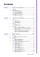
Contents Chapter 1 General Information ............................1 1.1 1.2 Introduction ............................................................................................... 2 Specifications ............................................................................................ 2 1.2.1 General Specification.................................................................... 2 1.2.2 Functional Specifications .............................................................. 3 1.2.
3.4.8 3.5 3.6 3.7 3.8 Chapter Embedded Controller Configuration ........................................... 23 Figure 3.10Embedded Controller Configuration ......................... 23 3.4.9 Super I/O Configuration .............................................................. 24 Figure 3.11Super IO Configuration............................................. 24 3.4.10 AOAC Configuration ................................................................... 25 Figure 3.12AOAC Configuration...................
Chapter 1 1 General Information
1.1 Introduction Advantech created the stackable architecture MI/O Extension Single Board Computer as a SBC design with flexible and multiple I/O support (hence the name MI/O) and united extended interface connector. MIO-5250 is a MI/O-Compact SBC (Single Board Computer) with Intel® Atom™ Cedar Trail ultra low power solution supporting up to 4GB 800/1066MHz DDR3, 6 USB2.0, SATAII (300 MBs), 4 COM and 2 GbE (up to 1000 Mbps). MIO-5250 supports dual displays, including VGA+LVDS, VGA+HDMI, and HDMI+LVDS.
RJ45 x2 Wake On Function Wake-on-LAN Display Intel® Atom N2600 / D2550 Controller Dual Independent Display VGA+LVDS, VGA+HDMI, HDMI+LVDS 1.2.2 Functional Specifications Processor: Intel® Atom N2600/D2550 CPU Process 32nm Frequency - N2600: 1.6GHz - D2550: 1.86GHz VGA Memory Up to 512MB of dynamic video memory allocation Internal Graphics Features Video Accelerator DirectX® 9 and OpenGL 3.0 Display Port 1.1, HDMI 1.3a Supports HDCP 1.
1.2.2.2 iManager iManager Sequence control Supported SMBus Supported GPIO 8-bit GPIO Watchdog timer Multi Level WDT (set by Advantech iManager) Programmable 1-255 sec / min Hardware monitor Input Voltage Power saving Deep sleep S5 mode/Back light control Board information Running HR / Boot record Storage Read / Write data protection VGA Low Level Backlight / Brightness control 1.2.2.
Chapter 1 1.2.4 Electrical Specifications 1.2.4.1 Power Supply Voltage Power Type Single 12V DC power in Power Supply Voltage Single 12V ± 10% Power Consumption (A) Condition Voltage/ Condition DOS Idle Mode Win. Idle Mode Win. HCT12 (10minutes) MIO-5250N-S6A1E +12V 0.606 0.524 0.729 MIO-5250D-S8A1E +12V 0.829 0.739 1.029 1.2.4.3 RTC Battery Typical Voltage: 3.0 V Normal discharge capacity: 210 mAh 1.2.5 Environmental Specifications 1.2.5.
1.3 Block Diagram Transmitter DisplayPort 1 48-bit LVDS2 18/24-bit LVDS1 Intel Atom N2600 / D2550 DDR3 SODIMM x 1 VGA I/F VGA DisplayPort 0 HDMI DMI (note1) Intel 82583V PCIe x 1 HD audio line out Intel 82583V PCIe x 1 COM1~COM4 (COM2/3: RS-232/422/485) (COM1/4: RS-232) Auto Flow Control Full-size MiniPCIe w/ SIM Holder 16MBit SPI BIOS USB 2.0 x 1 Super I/O LPC Intel NM10 MIOe SMBUS LPC PCIe x 1 1 PCIe x 1 SPI HD 6 USB 2.
Chapter 2 2 Hardware Installation
This chapter explains the setup procedures of the MIO-5250 A1 hardware, including instructions on setting jumpers and connecting peripherals, switches, indicators and mechanical drawings. Be sure to read all safety precautions before you begin the installation procedure. 2.1 Jumpers 2.1.1 Jumper List Table 2.1: Jumpers Label Function J1 24-bit LVDS1 Power J2 48-bit LVDS2 Power J3 Auto Power on setting J4 COM2 Setting J5 COM3 setting J6 Clear CMOS 2.1.
Chapter 2 Auto Power On Setting Part Number 1653002101 Footprint HD_2x1P_79_D Description PIN HEADER 2*1P 180D(M)SQUARE 2.0mm DIP W/O Pb Setting Function NC Power Button for Power On (1-2)* Auto Power On (default) J4 COM2 Setting Part Number 1653003260 Footprint HD_3x2P_79 Description PIN HEADER 3x2P 2.
(5-6) RS422 J6 Clear CMOS Part Number 1653003101 Footprint HD_3x1P_79_D Description PIN HEADER 3x1P 2.0mm 180D(M) DIP 2000-13 WS Setting Function (1-2)* Normal (default) (2-3) Clear COMS 2.1.3 Jumper Description Cards can be configured by setting jumpers. A jumper is a metal bridge used to close an electric circuit. It consists of two metal pins and a small metal clip (often protected by a plastic cover) that slides over the pins to connect them.
Warning! To avoid damaging the computer, always turn off the power supply before setting jumpers to clear CMOS. Before turning on the power supply, set the jumper back to 3.0 V Battery On. Hardware Installation 2.2 Connectors 2.2.1 Connector List Table 2.2: Connectors Label Function CN1 12V Power Input CN2 DC JACK CN3 DDR3 SO-DIMM CN5 Power Switch CN7 Reset CN9 GPIO CN10 VGA CN11 CFast CN12 SIM Holder Chapter 2 A pair of needle-nose pliers may be helpful when working with jumpers.
2.3 Mechanical 2.3.1 Jumper and Connector Location y CN22 CN20 CN14 p J6 CN15 CN26 CN34 CN7 CN5 CN38 J3 CN3 CN17 CN9 J2 CN33 J1 CN35 CN25 CN18 CN16 CN36 CN10 CN28 CN2 HDD& PWR LED Figure 2.1 Jumper and Connector Layout (Top Side) CN11 CN12 CN31 CN19 CN24 J4 J5 CN13 CN30 Figure 2.
Chapter 2 2.3.2 Board Dimensions Hardware Installation Figure 2.3 Board Dimensions (Component Side) Figure 2.
Figure 2.
Chapter 3 BIOS Settings 3
3.1 BIOS Setup AMIBIOS has been integrated into many motherboards for over a decade. With the AMIBIOS setup program, you can modify BIOS settings and control the various system features. This chapter describes the basic navigation of the MIO-5250 BIOS setup screens. Figure 3.1 Setup program initial screen AMI's BIOS ROM has a built-in Setup program that allows users to modify the basic system configuration.
When users first enter the BIOS Setup Utility, users will enter the Main setup screen. Users can always return to the Main setup screen by selecting the Main tab. There are two Main Setup options. They are described in this section. The Main BIOS Setup screen is shown below. Chapter 3 3.3 Main Setup BIOS Settings Figure 3.2 Main setup screen The Main BIOS setup screen has two main frames. The left frame displays all the options that can be configured.
3.4 Advanced BIOS Features Setup Select the Advanced tab from the MIO-5250 setup screen to enter the Advanced BIOS Setup screen. You can select any of the items in the left frame of the screen, such as CPU Configuration, to go to the sub menu for that item. You can display an Advanced BIOS Setup option by highlighting it using the keys. All Advanced BIOS Setup options are described in this section. The Advanced BIOS Setup screens are shown below. The sub menus are described on the following pages.
Chapter 3 3.4.2 ACPI Settings BIOS Settings Figure 3.4 ACPI Setting Enable ACPI Auto Configuration This item allows users to enable or disable BIOS ACPI auto configuration. Enable Hibernation This item allows users to enable or disable hibernation. ACPI Sleep State This item allows users to set the ACPI sleep state. Lock Legacy Resources This item allows users to lock legacy devices' resources. S3 Video Report This item allows users to enable or disable S3 resume for VBIOS.
3.4.3 TPM Configuration Figure 3.5 TPM Configuration TPM Support Disable/Enable TPM if available. 3.4.4 CPU Configuration Figure 3.
Hyper Threading Technology This item allows users to enable or disable Intel Hyper Threading technology. Execute Disable Bit This item allows users to enable or disable the No-Execution page protection Limit CPUID Maximum This item allows users to enable or disable limit CPUID maximum for Windows XP. Chapter 3 3.4.5 SATA Configuration BIOS Settings Figure 3.7 SATA Configuration SATA Controller(s) This item allows users to enable or disable the SATA controller(s).
3.4.6 Intel Fast Flash Standby Figure 3.8 Intel Fast Flash Standby IFFS Support This item allows users to enable or disable iFFS. 3.4.7 USB Configuration Figure 3.
3.4.8 Embedded Controller Configuration Figure 3.10 Embedded Controller Configuration EC iManager WatchDog IRQ This item allows users to set the IRQ number of EC watchdog. EC Power Saving Mode This item allows users to set board's power saving mode when off. Backlight Enable Polarity This item allows users to set backlight enable polarity. Backlight Mode This item allows users to set backlight mode. Backlight Mode 1 This item allows users to set backlight mode 1.
3.4.9 Super I/O Configuration Figure 3.11 Super IO Configuration Serial Port 0 Configuration This item allows users to configure serial port 0. Serial Port 1 Configuration This item allows users to configure serial port 1. Serial Port 2 Configuration This item allows users to configure serial port 2. Serial Port 3 Configuration This item allows users to configure serial port 3.
Chapter 3 3.4.10 AOAC Configuration BIOS Settings Figure 3.12 AOAC Configuration AOAC Configuration This item allows users to enable or disable AOAC function. 3.4.11 PPM Configuration Figure 3.
EIST This item allows users to enable or disable Intel SpeedStep function. CPU C state Report This item allows users to enable or disable CPU C state report to OS. Enhanced C state This item allows users to enable or disable Enhanced CPU C state. CPU Hard C4E This item allows users to enable or disable CPU Hard C4E function. CPU C6 state This item allows users to enable or disable CPU C6 state.
Chapter 3 3.5.1 Host Bridge/Intel IGD Configuration BIOS Settings Figure 3.15 Intel IGD Configuration Auto Disable IGD This item allows users to auto disable IGD upon external GFX detected. IGFX - Boot Type* This item allows users to select which output device during POST. LCD Panel Type This item allows users to select LCD panel by internal graphic device. Panel Scaling This item allows users to select LCD panel scaling by internal graphic device.
Boot type display Active_LFP CRT #No_LVDS NOTE LFP(LVDS1) #INT-LVDS EFP(HDMI) #No_LVDS It only supports Graphic Mode under DOS environment. EFP1(LVDS2) #LVDS 2 EFP1 will be item "built-in display" in driver device list CRT+LFP #INT-LVDS Dual Display is only supported with Graphic Mode under DOS environment. CRT+EFP #No_LVDS Dual Display is only supported with Graphic Mode under DOS environment. CRT+EFP1 #LVDS 2 Dual Display is only supported with Graphic Mode under DOS environment.
Chapter 3 BIOS Settings Figure 3.17 TPT Device Azalia Controller Enables or disables the azalia controller. Select USB Mode Select USB mode by controllers or ports. SMBus Controller Enables or disables the onchip SMBus controller. SIRQ Logic Enables or disables the SIRQ logic. SIRQ Mode Set SIRQ mode. MSATA/PCIe Switch Enables for MSATA disables for PCIe. LAN1/LAN2 Controller This item allows users to enables or disables LAN device.
3.6 Boot Settings Figure 3.18 Boot Setup Utility Setup Prompt Timeout This item allows users to select the number of seconds to wait for setup activation key. Bootup NumLock State Select the Power-on state for Numlock. Quiet Boot If this option is set to Disabled, the BIOS displays normal POST messages. If Enabled, an OEM Logo is shown instead of POST messages. Option ROM Message Set display mode for option ROM. Interrupt 19 Capture This item allows option ROMs to trap interrupt 19.
Chapter 3 3.7 Security Setup BIOS Settings Figure 3.19 Password Configuration Select Security Setup from the MIO-5250 Setup main BIOS setup menu. All Security Setup options, such as password protection is described in this section. To access the sub menu for the following items, select the item and press : Change Administrator / User Password Select this option and press to access the sub menu, and then type in the password.
3.8 Save & Exit Figure 3.20 Save & Exit 3.8.1 Save Changes and Exit When users have completed system configuration, select this option to save changes, exit BIOS setup menu and reboot the computer if necessary to take effect of all system configuration parameters. 3.8.2 Discard Changes and Exit Select this option to quit Setup without making any permanent changes to the system configuration. 3.8.
Select this option to discard any current changes and load previous system configuration. 3.8.7 Restore Defaults 3.8.8 Save User Defaults When users have completed system configuration, select this option to save changes as user defaults without exit BIOS setup menu. 3.8.9 Restore User Defaults The users can select this option to restore user defaults. 3.8.10 Boot Override You select device you want to do boot override.
MIO-5250 User Manual 34
Chapter 4 MIOe Installation 4
The MI/O compact form factor SBC is a new-generation SBC design with a variety of mechanical improvements. Here is the quick installation guide for our thermal design and MIOe module installation. Quick Installation Guide: 1. There is a Heatsink / Cooler in the white box inside the package. Carefully remove the release paper from the thermal pad before installation. Remove the release paper 2. 3.
Appendix A A Pin Assignments
CN1 12V Power Input Part Number 1655003865 Footprint WF_2x2P_165_BOX_RA_D_740SP Description Pin Pin Name 1 GND 2 GND 3 +12V 4 +12V CN2 DC JACK Part Number 1652005624 Footprint PJ_2P_2DC-G213B200 Description DC POWER JACK 2.5mm 90D(M) DIP 2DC-G213B200 Pin Pin Name 1 +VIN 2 GND CN3 SODIMMDDR3RVS_204 Part Number 1651001648 Footprint DDR3_204P_2-2013311-1 Description DDR3 SODIMM H=9.
Reset Part Number 1655302020 Footprint WF_2P_79_BOX_R1_D Description WAFER BOX 2P 2.0mm 180D(M) DIP A2001WV2-2P Pin Pin Name 1 RESET# 2 GND CN9 GPIO Part Number 1653004099 Footprint HD_5x2P_79_23N685B-10M10 Description BOX HEADER 5x2P 2.
CN10 VGA Part Number 1654000055 Footprint DBVGA-VF5MS Description D-SUB Conn. 15P 90D(F) DIP 070242FR015S200ZU Pin Pin Name 1 RED 2 GREEN 3 BLUE 4 NC 5 GND 6 GND 7 GND 8 GND 9 NC 10 GND 11 NC 12 DDAT 13 HSYNC 14 VSYNC 15 DCLK CN11 CFast Part Number 1653004849 Footprint CFAST_24P_N7G24 Description CFast 24P 1.
+3.3V PC14 +3.
CN13 Mini PCIE Part Number 1654006715 Footprint MINIPCI_52P_88911-5204M Description Pin Pin Name 1 WAKE# 2 +3.3VSB 3 NC 4 GND 5 NC 6 +1.5V 7 MINI_CLKREQ# 8 +VUIM_PWR 9 GND 10 UIM_DATA 11 REFCLK- 12 UIM_CLK 13 REFCLK+ 14 UIM_RESET 15 GND 16 +VUIM_VPP 17 NC 18 GND 19 NC 20 NC 21 GND 22 PERST# 23 PERn0 24 +3.3VSB 25 PERp0 26 GND 27 GND 28 +1.
NC 45 NC 46 NC 47 NC 48 +1.5V 49 NC 50 GND 51 NC 52 +3.
CN14 SATA Part Number 1654004118 Footprint SATA_7P_50_WATA-07DPLH4U Description Serial ATA 7P 1.27mm 90D(M) SMD WATA-07DPLH4U Pin Pin Name 1 GND 2 TX+ 3 TX- 4 GND 5 RX- 6 RX+ 7 GND CN15 SATA Power Part Number 1655001154 Footprint WF_4P_98_BOX_R1_D Description WAFER BOX 4P 2.
USB3/4 Part Number 1654009513 Footprint USB_8P_UB1112C-8FDE-4F Description USB CONN. 8P 2.0mm 90D DIP UB1112C-8FDE-4F Pin Pin Name 1 +5V 2 D- 3 D+ 4 GND CN17 Internal USB Part Number 1653005260 Footprint HD_5x2P_79_N10 Description PIN HEADER 2x5P 2.
CN18 USB 1/2 Part Number 1654009513 Footprint USB_8P_UB1112C-8FDE-4F Description USB CONN. 8P 2.0mm 90D DIP UB1112C-8FDE-4F Pin Pin Name 1 +5V 2 D- 3 D+ 4 GND CN19 COM1/COM2 RS-232 Part Number 1653004793 Footprint HD_10x2P_79_23N685B-20M10 Description BOX HEADER 10x2P 2.
CN20 RS422/485 1 Part Number 1655304032 Footprint WF_5P_49_BOX_85205 Description WAFER 5P 1.
CN22 RS422/485 2 Part Number 1655304032 Footprint WF_5P_49_BOX_85205 Description WAFER 5P 1.25mm 180D(M) SMD 85205-05701 Pin Pin Name 1 422RX- 2 422RX+ 3 422/485TX+ 4 422/485TX- 5 GND CN24 COM3/COM4 RS-232 Part Number 1653004793 Footprint HD_10x2P_79_23N685B-20M10 Description BOX HEADER 10x2P 2.
GND Matching Cable: 1701200220 CN25 SMBus Part Number 1655904020 Footprint FPC4V-125M Description WAFER 4P 1.25mm 180D(M) SMD 85205-04001 Pin Pin Name 1 GND 2 SMB_DAT 3 SMB_CLK 4 +5V CN26 System FAN Part Number 1655003010 Footprint WHP3VA Description Wafer 2.
CN28 LAN Part Number 1652003274 Footprint RJ45_28P_RTB-19GB9J1A Description PHONE JACK RJ45 28P DIP RTB-19GB9J1A Pin Pin Name 1 TX+(10/100), BI_DA+(GHz) 2 TX-(10/100), BI_DA-(GHz) 3 RX+(10/100), BI_DB+(GHz) 4 BI_DC+(GHz) 5 BI_DC-(GHz) 6 RX-(10/100), BI_DB-(GHz) 7 BI_DD+(GHz) 8 BI_DD-(GHz) CN30 Audio Part Number 1653004099 Footprint HD_5x2P_79_23N685B-10M10 Description BOX HEADER 5x2P 2.
MIOe Part Number 1654006235 Footprint BB_40x2P_32_1625x285_2HOLD Appendix A Pin Assignments CN31 Description Pin Pin Name 1 GND 2 GND 3 PCIE_RX0+ 4 PCIE_TX0+ 5 PCIE_RX0- 6 PCIE_TX0- 7 GND 8 GND 9 PCIE_RX1+ 10 PCIE_TX1+ 11 PCIE_RX1- 12 PCIE_TX1- 13 GND 14 GND 15 PCIE_RX2+ 16 PCIE_TX2+ 17 PCIE_RX2- 18 PCIE_TX2- 19 GND 20 GND 21 PCIE_RX3+ 22 PCIE_TX3+ 23 PCIE_RX3- 24 PCIE_TX3- 25 GND 26 GND 27 PCIE_CLK+ 28 LOUTL 29 PCIE_CLK- 30 LOUTR 31 GND
42 CLK33M 43 SLP_S5# 44 LPC_AD0 45 DDP_HPD 46 LPC_AD1 47 GND 48 LPC_AD2 49 DDP_AUX+ 50 LPC_AD3 51 DDP_AUX- 52 LPC_DRQ#0 53 GND 54 LPC_SERIRQ 55 DDP_D0+ 56 LPC_FRAME# 57 DDP_D0- 58 GND 59 GND 60 USB0_D+ 61 DDP_D1+ 62 USB0_D- 63 DDP_D1- 64 GND 65 GND 66 USB1_D+/USB_SSTX+ 67 DDP_D2+ 68 USB1_D-/USB_SSTX- 69 DDP_D2- 70 GND 71 GND 72 USB2_D+/USB_SSRX+ 73 DDP_D3+ 74 USB2_D-/USB_SSRX- 75 DDP_D3- 76 GND 77 GND 78 USB_OC# 79 +12VSB 80 NC 83
Appendix A Pin Assignments CN33 24 bits LVDS1 Panel Part Number 1653910261 Footprint SPH10X2 Description B/B Conn 10x2P 1.25mm 180D(M)SMD DF13-20DP-1.
12 NC 13 LVDS0_D2- 14 NC 15 LVDS0_CLK+ 16 LVDS0_D3+ 17 LVDS0_CLK- 18 LVDS0_D3- 19 +5V or +3.3V 20 +5V or +3.3V CN34 48 bits LVDS2 Inverter Power Part Number 1655000453 Footprint WHL5V-2M-24W1140 Description WAFER BOX 2.
48 bits LVDS2 Panel Part Number 1653920200 Footprint SPH20X2 Description B/B Conn. 40P 1.25mm 90D SMD DF13-40DP-1.25V(91) Pin Pin Name 1 +5V or +3.3V 2 +5V or +3.3V 3 GND 4 GND 5 +5V or +3.3V 6 +5V or +3.
CN36 HDMI Part Number 1654009225 Footprint HDMI_19P_QJ51193-FFD4-7F Description HDMI Conn 19P 0.
eDP Part Number 1653910261 Footprint SPH10X2 Description B/B Conn 10x2P 1.25mm 180D(M)SMD DF13-20DP-1.25V Pin Pin Name 1 GND 2 GND 3 D0- 4 D3- 5 D0+ 6 D3+ 7 GND 8 NC 9 D1- 10 GND 11 D1+ 12 SDAT 13 GND 14 SCLK 15 D2- 16 GND 17 D2+ 18 Hot Plug Detect 19 +5V or +3.3V 20 +5V or +3.
CN38 24 bits LVDS1 Inverter Power Part Number 1655000453 Footprint WHL5V-2M-24W1140 Description WAFER BOX 2.
Appendix B B System Assignments
B.1 System I/O Ports Table B.1: System I/O Ports Addr.
Table B.3: 1st MB memory map Addr. Range (Hex) Device E0000h - FFFFFh System board D0000h - DFFFFh PCI Bus C0000h - CFFFFh System board A0000h - BFFFFh PCI Bus A0000h - BFFFFh Intel® HD Graphic 00000h - 9FFFFh System board B.4 Interrupt assignments Table B.
MIO-5250 User Manual 62
Appendix C Watchdog Timer Sample Code C
C.1 EC Watchdog Timer sample code EC_Command_Port = 0x29Ah EC_Data_Port = 0x299h Write EC HW ram = 0x89 Watch dog event flag = 0x57 Watchdog reset delay time = 0x5E Reset event = 0x04 Start WDT function = 0x28 ==================================================== .model small .486p .stack 256 .data .code org 100h .STARTup mov dx, EC_Command_Port mov al,89h ; Write EC HW ram. out dx,al mov dx, EC_Command_Port mov al, 5Fh ; Watchdog reset delay time low byte (5Eh is high byte) index.
Appendix C Watchdog Timer Sample Code MIO-5250 User Manual 65
www.advantech.com Please verify specifications before quoting. This guide is intended for reference purposes only. All product specifications are subject to change without notice. No part of this publication may be reproduced in any form or by any means, electronic, photocopying, recording or otherwise, without prior written permission of the publisher. All brand and product names are trademarks or registered trademarks of their respective companies. © Advantech Co., Ltd.