
User manual
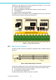
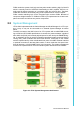
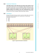


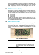
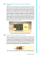
Table Of Contents
- UTCA-5503
- Contents
- 1 Board Specification
- 2 Applications and Overview
- 3 Mezzanine Module Options
- 4 Operations
- 5 Firmware Upgrades
- 6 Overview of Supported Features and Known Limitations
- A MCH Pin List, Connector 1
- B IPMI/PICMG Command Subset Supported by the MCMC
- C IPMI/PICMG Command Subset Supported by the Carrier Manager
- D IPMI/PICMG Command Subset Supported by the uShM
17 UTCA-5503 User Manual
Chapter 3 Mezzanine Module Options
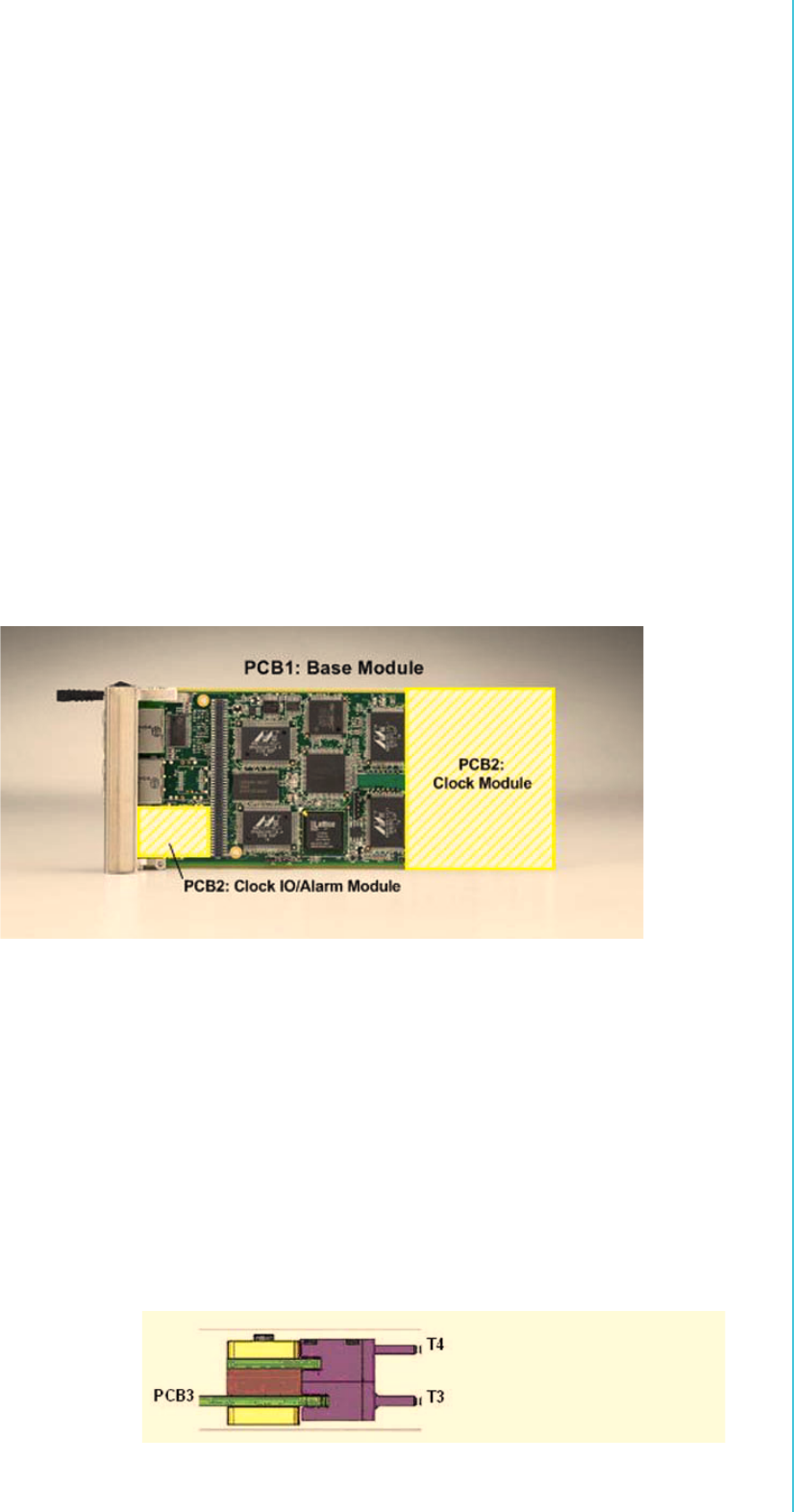
3.3 Clock Module and Clock IO/Alarm Module
(PCB2)
PCB2 can consist of two mezzanines - a Clock IO/Alarm Module and a Clock Module
(see Figure 3.2). The Clock IO/Alarm Module contains the interfaces or ports for
multi-carrier/shelf clock distribution and synchronization (daisy chain cabling sup-
ported) as well as external reference clock receptions such as GPS derived clocks,
BITS clocks, or other general purpose clocks. Up to two SMA connectors can be
implemented on the front panel of the module. The Clock Module can be designed
with various clock generator options for synchronous network system applications
such as distribution of accurate timing at Stratum 2 from Stratum 1, Stratum 3 from
Stratum 2, or Stratum 4 from Stratum2/3. In addition, it can provide clock transmitters/
receivers, multiplexers, and routing functionalities for the AMC modules, the other
MCH, and the Clock IO/Alarm Module. Two high-speed differential clocks can be
interfaced between the Clock Module and PCB3 (fabric switch) with the input being
driven by PCB3 and the output being driven by the Clock Module. Fabric clock deliv-
ered to the AMC’s or vice versa is interfaced through the Clock Module. Fabric clock
delivered to “the outside” world is also interfaced through the Clock Module with the
Clock IO/Alarm Module working as the output.
Figure 3.2 Illustration of PCB2 location relative to PCB1
3.4 Fabric Extension Module (PCB3)
PCB3 is a fabric extension module of MCH PCB1. Its purpose is to provide fat pipes
switching capabilities for PCIe protocol. Each MCH connects to the AMCs with 4
channels each in a Star topology and to the second MCH with 4 channels. Such logic
is considered to be in the payload domain. E-keying is implemented by I2C configu-
ration bus connected on the MCMC through a buffer. There are two high speed differ-
ential clocks connecting to the Clock Module to support high speed clock distribution,
especially in spread spectrum environments. PCB3 will implement a MCH tongue 3
and 4 connector to reduce the mating force for the MCH. See Figure 3.3 for illustra-
tion. The PCIe switch based PCB3 for UTCA-5503 is called UTCA-5533.
Figure 3.3 Connection between Tongue 3 and Tongue 4 (Yamaichi MCH plug)