
Specifications
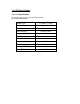
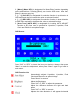
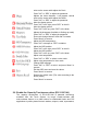

1.4.2 LCD pin definition
M150XN07 pin definition is shown in the table below.
1 VDD Power Supply, 3.3V (typical)
2 VDD Power Supply, 3.3V (typical)
3 VSS Ground
4 VSS Ground
5 Rin0- - LVDS differential data input (R0-R5, G0)
6 Rin0+ + LVDS differential data input (R0-R5, G0)
7 VSS Ground
8 Rin1- - LVDS differential data input (G1-G5, B0-B1)
9 Rin1+ + LVDS differential data input (G1-G5, B0-B1)
10 VSS Ground
11 Rin2- - LVDS differential data input (B2-B5, HS, VS, DE)
12 Rin2+ + LVDS differential data input (B2-B5, HS, VS, DE)
13 VSS Ground
14 ClkIN- - LVDS differential clock input
15 ClkIN+ + LVDS differential clock input
16 VSS Ground
17 Rin3- NC
18 Rin3+ NC
19 VSS Ground
20 NC NC Please *floating* and don’t connect to ground.