
User's Manual


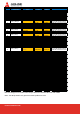

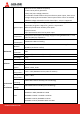
Table Of Contents

DOC#NCP-R4600 GEN2-SOW
Remark: background in amber show the pin difference between MC7445 and LM960
Note : Pin 28 Dip Switch only present on Mass production units
Pin #
mPCIe slot 5 & 6
USB 2.0+PCIe x1
mPCIe slot 3 & 4
USB 3.0
Sierra MC7455
module
Telit LM960
module
Notes
Location
AFM
AFM
-- --
1
MPCIE_5_WAKE_N
Module define
WAKE#
NC
2
P3V3_SB_MPCIE_5
3V3 VCC VBATT
3
NC
NC ANT_CTRL0/GPIO1 GPIO_01
4
GND
GND GND GND
5
NC
NC ANT_CTRL1/GPIO2 GPIO_02
6
P1V5_MPCIE_5
NC NC NC
7
MPCIE_5_CLKREQ_N
NC USIM2_RST PCIE_CLKREQ_N*
*datasheet r7 Information – PCIe bus
is currently NOT supported, PCI pins
marked with * are for future use only
8
MODEM_SIM5_VSIM
SIM1_PWR
USIM_PWR
SIMVCC1
9
GND
GND GND GND
10
MODEM_SIM5_DAT
SIM1_DAT USIM_DATA SIMIO1
11
MPCIE_5_CLK_R_N
Module define VREF_1.8V PCIE_REFCLK_M*
*datasheet r7 Information – PCIe bus
is currently NOT supported, PCI pins
marked with * are for future use only
12
MODEM_SIM5_CLK
SIM1_CLK
USIM_CLK
SIMCLK1
13
MPCIE_5_CLK_R_P
NC USIM2_PWR PCIE_REFCLK_P*
*datasheet r7 Information – PCIe bus
is currently NOT supported, PCI pins
marked with * are for future use only
14
MODEM_SIM5_RST
SIM1_RST
USIM_RST SIMRST1
15
GND
GND GND GND
16
NC
NC NC SIMVCC2
17
NC
NC USIM2_CLK SIMCLK2
18
GND
GND GND GND
19
NC
NC USIM2_DATA SIMIO2
20
MPCIE_5_W_DISABLE_L
W1_DISABLE_N(TP) W_DISABLE# W_DISABLE_N
21
GND
GND GND GND
22
MPCIE_5_PERST_N
DIP switch SYSTEM_RESET#
PCIE_RESET_N*
*datasheet r7 Information – PCIe bus
is currently NOT supported, PCI pins
marked with * are for future use only
23
AFM_PCIE_RX1_N
U3P1_RXN
USB3.0_TX- USB_SS_TX_M
24
P3V3_SB_MPCIE_5
3V3 VCC VBATT
25
AFM_PCIE_RX1_P
U3P1_RXP USB3.0_TX+ USB_SS_TX_P
26
GND
GND GND GND
27
GND
GND GND GND
28
P1V5_MPCIE_5
DIP switch NC VREG_L6_1P8
DIP switch for P1.5V and NC options
29
GND
GND GND
GND
30
MPCIE_5_SMB_LS_CLK
NC NC I2C_SCL
31
AFM_PCIE_TX1_N
U3P1_TXN USB3.0_RX- USB_SS_RX_M
32
MPCIE_5_SMB_LS_DAT
NC NC I2C_SDA
33
AFM_PCIE_TX1_P
U3P1_TXP USB3.0_RX+ USB_SS_RX_P
34
GND
GND GND GND
35
GND
GND GND GND
36
MPCIE_5_USB2_N
USB-N2_C USB_D- USB_D-
37
GND
GND GND GND
38
MPCIE_5_USB2_P
USB-P2_C USB_D+ USB_D+
39
P3V3_SB_MPCIE_5
3V3 VCC VBATT
40
GND
GND GND GND
41
P3V3_SB_MPCIE_5
3V3 VCC VBATT
42
MPCIE_5_LED_WWAN_N
MPCIE_2_LED_WWAN_N WAN_LED# WAN_LED_N
43
GND
GND GND GND
44
NC
NC ANT_CTRL2/GPIO3 GPIO_03
45
NC
NC NC GPIO_05
46
NC
NC DPR/GPIO4 GPIO_04
47
NC
NC NC GPIO_06
48
P1V5_MPCIE_5
DIP switch NC SYSTEM_RESET_N
49
NC
NC NC GPIO_07
50
GND
GND GND GND
51
NC
NC NC GPIO_08
52
P3V3_SB_MPCIE_5
3V3 VCC VBATT