
User`s manual

Jumpers and Connectors • 25
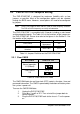
2.3 PXD-3710/3710F Jumpers Setting
The PXD-3710/3710F is designed for maximum flexibility with as few
jumpers as possible. Most of the configuration options can be selected
through the BIOS menu. However, some options still need to be configured
by jumpers.
Note. There is no jumper for front side bus (FSB) or CPU frequency selection.
The FSB and CPU frequency are set by auto-detection.
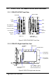
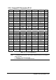
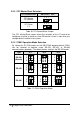
The PXD-3710/3710F is assembled with 3 boards including a main board
and two daughter boards. The Table 14 lists the functions of the jumpers on
the PXD-3710/3710F. Please also refer to the figures in the Section 2.1 for
the location of the jumpers.
Description Location Name
Clear CMOS
PXD-3710/3710F
Main board
JP1
CF1 Master/Slave Selection DB-3710L2 CN7
COM1 RS232/422/RS485
Selection
DB-3710L3 JP1~3
Table 14: Jumpers Definition on the PXD-3710/3710F
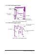
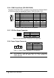
2.3.1 Clear CMOS
RTC status PXD-3710 JP1
Normal operation
1-2 (Default)
Clear CMOS
2-3
Table 15: Clear CMOS RTC RAM
The CMOS RAM data for real time clock (RTC) contains the date / time and
password information. The CMOS is powered by the button cell-battery when
the system is power-off.
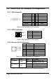
To erase the CMOS RAM data:
1. Unplug the PXD-3710/3710F.
2. Short pins 2 and 3 of JP1. Then reinstall the jumper back to
normal location.
3. Plug the PXD-3710/3710F back to the chassis. Turn the power
on.
3 2 1
3 2 1