
User`s manual

8 • Introduction
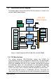
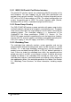
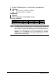
1.3 Functional Block Diagram
The following topics overview the PXD-3710 main features as shown in the
functional block diagram below.
CPU
Socket-370
Intel 815E
GMCH2
Intel 82801
ICH2
W83627 SIO
SO-DIMM
X2
USB x2
USB to
Compact
Flash2
PS2
KB/MS
PRT,COM1
VGA
IDE2
Compact
Flash 1
LEDs
Front Panel
(3 or 4 Slot)
USB x1
COM2
DVO
DVO to DVI
CH7301
DVO to LVDS
DS90C387R
IDE1
HW
monitor
100/133MHz
Compact PCI J
2
Compact PCI J
1
Rear IO
PCI 32/33
Clock
Generator
PXD-3710
Block Diagram
PWM
LVDS to FPD
DS90CF384A
PXD-R3000
FLOPPY
(optional)
Figure 1: Block Diagram of PXD-3710/3710F and PXD-R3000
1.3.1 PXI Bus Interface
The system controller PXD-3710/3710F follows the PICMG 2.8
Instrumentation Extensions to CompactPCI specifications. PXI specifications
dedicate the leftmost slot of the PXI chassis to the system controller. PXI is
electrically compatible with the PCI bus standard, and provides enhanced
instrumentation signals for synchronization or communication between
peripherals. Based on the mechanical design of CompactPCI systems, PXI
systems can work in harsh, shocking, and high temperature environments.
The PXD-3710/3710F utilizes a 32-bit/33MHz PCI bus. The 64-bit PCI
signals on the PXI J2 connector are not used and therefore reserved for rear